

Active Member
|
[China]

Address: #506B, Henghui Business Center, No.77, Lingxia Nan Road, High Technology Zone, Huli, Xiamen 361006, China
Contact name:

XIAMEN POWERWAY ADVANCED MATERIAL CO., LTD. |
|
|
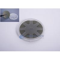
4H N Type SiC(Silicon Carbide) Lapping Wafer, 4”Size - Powerway Wafer
PAM-XIAMEN offers semiconductor silicon carbide wafers,6H SiC and 4H SiC in different quality grades for researcher and industry manufacturers. We has developed SiC crystal growth technology and SiC crystal wafer processing technology,established a production line to manufacturer SiCsubstrate,Which is applied in GaNepitaxydevice,powerdevices,high-temperature device and optoelectronic Devices. As a professional company invested by the leading manufacturers from the fields of advanced and high-tech material research and state institutes and China’s Semiconductor Lab,weare devoted to continuously improve the quality of currently substrates and develop large size substrates.
Here shows detail specification::
SILICON CARBIDE MATERIAL PROPERTIES
| Polytype | Single Crystal 4H | Single Crystal 6H |
| Lattice Parameters | a=3.076 Å | a=3.073 Å |
| c=10.053 Å | c=15.117 Å | |
| Stacking Sequence | ABCB | ABCACB |
| Band-gap | 3.26 eV | 3.03 eV |
| Density | 3.21 · 103 kg/m3 | 3.21 · 103 kg/m3 |
| Therm. Expansion Coefficient | 4-5×10⁻⁶/K | 4-5×10⁻⁶/K |
| Refraction Index | no = 2.719 | no = 2.707 |
| ne = 2.777 | ne = 2.755 | |
| Dielectric Constant | 9.6 | 9.66 |
| Thermal Conductivity | 490 W/mK | 490 W/mK |
| Break-Down Electrical Field | 2-4 · 108 V/m | 2-4 · 108 V/m |
| Saturation Drift Velocity | 2.0 · 105 m/s | 2.0 · 105 m/s |
| Electron Mobility | 800 cm2/V·S | 400 cm2/V·S |
| hole Mobility | 115 cm2/V·S | 90 cm2/V·S |
| Mohs Hardness | ~9 | ~9 |
4H N Type SiC Lapping Wafer, 4”Size
| 4" 4H Silicon Carbide | |||||||
| Item No. | Type | Orientation | Thickness | Grade | Micropipe Density | Surface | Usable area |
| N-Type | |||||||
| S4H-100-N-SIC-350-A | 4" 4H-N | 0°/4°±0.5° | 350±25um | A | <10/cm2 | P/P | >90% |
| S4H-100-N-SIC-350-B | 4" 4H-N | 0°/4°±0.5° | 350±25um | B | < 30/cm2 | P/P | >85% |
| S4H-100-N-SIC-350-D | 4" 4H-N | 0°/4°±0.5° | 350±25um | D | <100/cm2 | P/P | >75% |
| S4H-100-N-SIC-370-L | 4" 4H-N | 0°/4°±0.5° | 370±25um | D | * | L/L | >75% |
| S4H-100-N-SIC-440-AC | 4" 4H-N | 0°/4°±0.5° | 440±25um | D | * | As-cut | >75% |
| S4H-100-N-SIC-C0510-AC-D | 4" 4H-N | 0°/4°±0.5° | 5~10mm | D | <100/cm2 | As-cut | * |
| S4H-100-N-SIC-C1015-AC-C | 4" 4H-N | 0°/4°±0.5° | 5~10mm | C | <50/cm2 | As-cut | * |
SiC crystal growth
Bulk crystal growth is the technique for fabrication of single crystalline substrates , making the base for further device processing.To have a breakthrough in SiC technology obviously we need production of SiC substrate with a reproducible process.6H- and 4H- SiC crystals are grown in graphite crucibles at high temperatures up to 2100—2500°C. The operating temperature in the crucible is provided either by inductive (RF) or resistive heating. The growth occurs on thin SiC seeds. The source represents polycrystalline SiC powder charge. The SiC vapor in the growth chamber mainly consists of three species, namely, Si, Si2C, and SiC2, which are diluted by carrier gas, for example, Argon. The SiC source evolution includes both time variation of porosity and granule diameter and graphitization of the powder granules.
SiC Insulators: Thermal Oxides and MOS Technology
The vast majority of semiconductor-integrated circuit chips in use today rely on silicon metal-oxide–
semiconductor field-effect transistors (MOSFETs), whose electronic advantages and operational
device physics are summarized in Katsumata’s chapter and elsewhere . Given the extreme
usefulness and success of inversion channel MOSFET-based electronics in VLSI silicon (as well as
discrete silicon power devices), it is naturally desirable to implement high-performance inversion
channel MOSFETs in SiC. Like silicon, SiC forms a thermal ![]() when it is sufficiently heated in an
when it is sufficiently heated in an
oxygen environment. While this enables SiC MOS technology to somewhat follow the highly successful
path of silicon MOS technology, there are nevertheless important differences in insulator quality and
device processing that are presently preventing SiC MOSFETs from realizing their full beneficial
potential. While the following discourse attempts to quickly highlight key issues facing SiC MOSFET
development, more detailed insights can be found in References 133–142.
From a purely electrical point of view, there are two prime operational deficiencies of SiC oxides and
MOSFETs compared to silicon MOSFETs. First, effective inversion channel mobilities in most SiC MOSFETs
are lower than one would expect based on silicon inversion channel MOSFET carrier mobilities.
This seriously reduces the transistor gain and current-carrying capability of SiC MOSFETs, so that SiC
MOSFETs are not nearly as advantageous as theoretically predicted. Second, SiC oxides have not proven
as reliable and immutable as well-developed silicon oxides, in that SiC MOSFETs are more prone to
threshold voltage shifts, gate leakage, and oxide failures than comparably biased silicon MOSFETs. In
particular, SiC MOSFET oxide electrical performance deficiencies are attributed to differences between
silicon and SiC thermal oxide quality and interface structure that cause the SiC oxide to exhibit undesirably
higher levels of interface state densities (![]() ), fixed oxide charges (
), fixed oxide charges (![]() ),
),
charge trapping, carrier oxide tunneling, and lowered mobility of inversion channel carriers.
In highlighting the difficulties facing SiC MOSFET development, it is important to keep in mind that
early silicon MOSFETs also faced developmental challenges that took many years of dedicated research
efforts to successfully overcome. Indeed, tremendous improvements in 4H-SiC MOS device performance
have been achieved in recent years, giving hope that beneficial 4H-SiC power MOSFET devices for
operation up to 125°C ambient temperatures might become commercialized within the next few years.
For example, 4H-SiC MOSFET inversion channel mobility for conventionally oriented (8° off (0001)
c-axis) wafers has improved from <10 to >200 ![]() , while the density of electrically detrimental
, while the density of electrically detrimental
SiC–![]() interface state defects energetically residing close to the
conduction band edge has dropped by
interface state defects energetically residing close to the
conduction band edge has dropped by
an order of magnitude . Likewise, alternative SiC wafer surface
orientations such as (![]() )
)
and ( ![]() ) that are obtained by making devices on wafers cut with different
crystallographic orientations
) that are obtained by making devices on wafers cut with different
crystallographic orientations
(Section 5.2.1), have also yielded significantly improved 4H-SiC MOS channel properties .
One key step to obtaining greatly improved 4H-SiC MOS devices has been the proper introduction
of nitrogen-compound gases (in the form of ![]() ) during the oxidation and postoxidation
) during the oxidation and postoxidation
annealing process . These nitrogen-based anneals have also improved the
stability of 4H-SiC oxides to high electric field and high-temperature stressing used to qualify and
quantify the reliability of MOSFETs . However, as Agarwal et al. have pointed out, the wide
bandgap of SiC reduces the potential barrier impeding tunneling of damaging carriers through oxides
grown on 4H-SiC, so that 4H-SiC oxides cannot be expected to attain identical high reliability as
thermal oxides on silicon. It is highly probable that alternative gate insulators besides thermally grown
![]() will have to be developed for optimized implementation of
inversion channel 4H-SiC insulated
will have to be developed for optimized implementation of
inversion channel 4H-SiC insulated
gate transistors for the most demanding high-temperature and high-power electronic applications. As
with silicon MOSFET technology, multilayer dielectric stacks will likely be developed to further enhance
SiC MOSFET performance .
 Lapping Wafer, 4”Size - Powerway Wafer")
 Lapping Wafer, 4”Size - Powerway Wafer")
 Lapping Wafer, 4”Size - Powerway Wafer")
 Lapping Wafer, 4”Size - Powerway Wafer")
 Lapping Wafer, 4”Size - Powerway Wafer")
 Lapping Wafer, 4”Size - Powerway Wafer")