

Active Member
|
[China]

Address: #506B, Henghui Business Center, No.77, Lingxia Nan Road, High Technology Zone, Huli, Xiamen 361006, China
Contact name:

XIAMEN POWERWAY ADVANCED MATERIAL CO., LTD. |
|
|
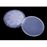
Semi-Insulating , GaAs Wafer With Low Defect Density , 3”, Prime Grade
PAM-XIAMEN develops and manufactures compound semiconductor substrates-gallium arsenide crystal and wafer.We has used advanced crystal growth technology,vertical gradient freeze(VGF) and GaAs wafer processing technology,established a production line from crystal growth, cutting, grinding to polishing processing and built a 100-class clean room for wafer cleaning and packaging. Our GaAs wafer include 2~6 inch ingot/wafers for LED,LD and Microelectronics applications. We are always dedicated to improve the quality of currently substates and develop large size substrates.
(GaAs)Gallium Arsenide Wafers,Semi-insulating for Microelectronics Applications
| Item | Specifications | Remarks |
| Conduction Type | Insulating | |
| Growth Method | VGF | |
| Dopant | Undoped | |
| Wafer Diamter | 3, inch | Ingot available |
| Crystal Orientation | (100)+/- 0.5° | |
| OF | EJ, US or notch | |
| Carrier Concentration | n/a | |
| Resistivity at RT | >1E7 Ohm.cm | |
| Mobility | >5000 cm2/V.sec | |
| Etch Pit Density | <8000 /cm2 | |
| Laser Marking | upon request | |
| Surface Finish | P/P | |
| Thickness | 350~675um | |
| Epitaxy Ready | Yes | |
| Package | Single wafer container or cassette | |
Properties of GaAs Crystal
| Properties | GaAs |
| Atoms/cm3 | 4.42 x 10²² |
| Atomic Weight | 144.63 |
| Breakdown Field | approx. 4 x 10⁵ |
| Crystal Structure | Zincblende |
| Density (g/cm3) | 5.32 |
| Dielectric Constant | 13.1 |
| Effective Density of States in the Conduction Band, Nc (cm-3) | 4.7 x 10¹⁷ |
| Effective Density of States in the Valence Band, Nv (cm-3) | 7.0 x 10¹⁸ |
| Electron Affinity (V) | 4.07 |
| Energy Gap at 300K (eV) | 1.424 |
| Intrinsic Carrier Concentration (cm-3) | 1.79 x 10⁶ |
| Intrinsic Debye Length (microns) | 2250 |
| Intrinsic Resistivity (ohm-cm) | 108 |
| Lattice Constant (angstroms) | 5.6533 |
| Linear Coefficient of Thermal Expansion, | 6.86 x 10⁻⁶ |
| ΔL/L/ΔT (1/deg C) | |
| Melting Point (deg C) | 1238 |
| Minority Carrier Lifetime (s) | approx. 10-8 |
| Mobility (Drift) | 8500 |
| (cm2/V-s) | |
| µn, electrons | |
| Mobility (Drift) | 400 |
| (cm2/V-s) | |
| µp, holes | |
| Optical Phonon Energy (eV) | 0.035 |
| Phonon Mean Free Path (angstroms) | 58 |
| Specific Heat | 0.35 |
| (J/g-deg C) | |
| Thermal Conductivity at 300 K | 0.46 |
| (W/cm-degC) | |
| Thermal Diffusivity (cm2/sec) | 0.24 |
| Vapor Pressure (Pa) | 100 at 1050 deg C; |
| 1 at 900 deg C |
| Wavelength | Index |
| (µm) | |
| 2.6 | 3.3239 |
| 2.8 | 3.3204 |
| 3 | 3.3169 |
| 3.2 | 3.3149 |
| 3.4 | 3.3129 |
| 3.6 | 3.3109 |
| 3.8 | 3.3089 |
| 4 | 3.3069 |
| 4.2 | 3.3057 |
| 4.4 | 3.3045 |
| 4.6 | 3.3034 |
| 4.8 | 3.3022 |
| 5 | 3.301 |
| 5.2 | 3.3001 |
| 5.4 | 3.2991 |
| 5.6 | 3.2982 |
| 5.8 | 3.2972 |
| 6 | 3.2963 |
| 6.2 | 3.2955 |
| 6.4 | 3.2947 |
| 6.6 | 3.2939 |
| 6.8 | 3.2931 |
| 7 | 3.2923 |
| 7.2 | 3.2914 |
| 7.4 | 3.2905 |
| 7.6 | 3.2896 |
| 7.8 | 3.2887 |
| 8 | 3.2878 |
| 8.2 | 3.2868 |
| 8.4 | 3.2859 |
| 8.6 | 3.2849 |
| 8.8 | 3.284 |
| 9 | 3.283 |
| 9.2 | 3.2818 |
| 9.4 | 3.2806 |
| 9.6 | 3.2794 |
| 9.8 | 3.2782 |
| 10 | 3.277 |
| 10.2 | 3.2761 |
| 10.4 | 3.2752 |
| 10.6 | 3.2743 |
| 10.8 | 3.2734 |
| 11 | 3.2725 |
| 11.2 | 3.2713 |
| 11.4 | 3.2701 |
| 11.6 | 3.269 |
| 11.8 | 3.2678 |
| 12 | 3.2666 |
| 12.2 | 3.2651 |
| 12.4 | 3.2635 |
| 12.6 | 3.262 |
| 12.8 | 3.2604 |
| 13 | 3.2589 |
| 13.2 | 3.2573 |
| 13.4 | 3.2557 |
| 13.6 | 3.2541 |
What is a GaAs Test Wafer?
Most GaAs test wafers are wafers which have fallen out of prime specifications. Test wafers may be used to run marathons, test equipment and for high-end R & D. They are often a cost-effective alternative to prime wafers.
What is the Basic Parameters at 300 K of GaAs Wafer?
| Crystal structure | Zinc Blende |
| Group of symmetry | Td2-F43m |
| Number of atoms in 1 cm3 | 4.42·1022 |
| de Broglie electron wavelength | 240 A |
| Debye temperature | 360 K |
| Density | 5.32 g cm-3 |
| Dielectric constant (static ) | 12.9 |
| Dielectric constant (high frequency) | 10.89 |
| Effective electron mass me | 0.063mo |
| Effective hole masses mh | 0.51mo |
| Effective hole masses mlp | 0.082mo |
| Electron affinity | 4.07 eV |
| Lattice constant | 5.65325 A |
| Optical phonon energy | 0.035 eV |
Are You Looking for GaAs Wafer?
PAM-XIAMEN is your go-to place for everything wafers, including GaAs wafers, as we have been doing it for almost 30 years! Enquire us today to learn more about the wafers that we offer and how we can help you with your next project. Our group team is looking forward to providing both quality products and excellent service for you!


