

Active Member
|
[China]

Address: #506B, Henghui Business Center, No.77, Lingxia Nan Road, High Technology Zone, Huli, Xiamen 361006, China
Contact name:

XIAMEN POWERWAY ADVANCED MATERIAL CO., LTD. |

|
|
N Type , Indium Phosphide Wafer , 6”, Test Grade -Powerway Wafer
PAM-XIAMEN provides single crystal InP(Indium phosphide) wafer for micro-electronic ( HBT/ HEMT ) and opto-electronic industry ( LED / DWDM / PIN / VCSELs ) in diameter up to 6 inch. Indium phosphide ( InP ) crystal is formed by two elements , Indium and Phosphide , growth by Liquid Encapsulated Czochralski ( LEC ) method or VGF method . InP wafer is an important semiconductor material which have superior electrical and thermal properties, InP wafer has higher electron mobility, higher frequency, low power consumption , higher thermal conductivity and low noise performance . PAM-XIAMEN can provide epi ready grade InP wafer for your MOCVD & MBE epitaxial application .Please contact our engineer team for more wafer information.
N Type, Indium Phosphide Wafer, 6”, Test Grade
| 6"InP Wafer Specification | ||||
| Item | Specifications | |||
| Conduction Type | N-type | N-type | ||
| Dopant | Undoped | Sulphur | ||
| Wafer Diameter | 6" | |||
| Wafer Orientation | 100±0.5° | |||
| Wafer Thickness | ||||
| Primary Flat Length | ||||
| Secondary Flat Length | ||||
| Carrier Concentration | ≤3x1016cm-3 | (0.8-6)x1018cm-3 | (0.6-6)x1018cm-3 | N/A |
| Mobility | (3.5-4)x103cm2/V.s | (1.5-3.5)x103cm2/V.s | 50-70cm2/V.s | >1000cm2/V.s |
| Resistivity | N/A | N/A | N/A | >0.5x10⁷Ω.cm |
| EPD | <1000cm-2 | <1x103cm-2 | <1x103cm-2 | <5x103cm-2 |
| TTV | ||||
| BOW | ||||
| WARP | ||||
| Laser Marking | upon request | |||
| Suface Finish | P/E, P/P | |||
| Epi Ready | yes | |||
| Package | Single wafer container or cassette | |||
Indium Phosphide Facts
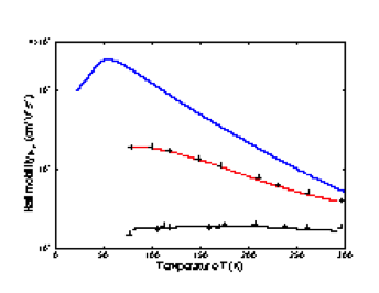 | Electron Hall mobility versus temperature for different doping
levels. Bottom curve - no=Nd-Na=8·1017 cm-3; Middle curve - no=2·1015 cm-3; Top curve - no=3·1013 cm-3. (Razeghi et al. [1988]) and (Walukiewicz et al [1980]). |
 | Electron Hall mobility versus temperature (high temperatures): Bottom curve - no=Nd-Na~3·1017 cm-3; Middle curve - no~1.5·1016 cm-3; Top curve - no~3·1015 cm-3. (Galavanov and Siukaev[1970]). |
µn = (4.2÷5.4)·103·(300/T) (cm2V-1 s-1)
 | Hall mobility versus electron concentration for different
compensation ratios. θ = Na/Nd, 77 K. Dashed curves are theoretical calculations: 1. θ = 0; 2. θ = 0.2; 3. θ = 0.4; 4. θ = 0.6; 5. θ = 0.8; (Walukiewicz et al. [1980]). Solid line is mean observed values (Anderson et al. [1985]). |
 | Hall mobility versus electron concentration for different
compensation ratios θ =Na/Nd, 300 K. Dashed curves are theoretical calculations: 1. θ = 0; 2. θ = 0.2; 3. θ = 0.4; 4. θ = 0.6; 5. θ = 0.8; (Walukiewicz et al. [1980]). Solid line is mean observed values (Anderson et al. [1985]). |
µ=µOH/[1+(Nd/107)1/2],
where µOH=5000 cm2V-1 s-1,
Nd- in cm-3 (Hilsum [1974])
At 300 K, the electron Hall factor rn≈1 in n-InP.
for Nd > 1015 cm-3.
 | Hole Hall mobility versus temperature for different doping (Zn)
levels. Hole concentration at 300 K: 1. 1.75·1018 cm-3; 2. 3.6·1017 cm-3; 3. 4.4·1016 cm-3. θ=Na/Nd~0.1. (Kohanyuk et al. [1988]). |
µpH~150·(300/T)2.2 (cm2V-1 s-1).
 | Hole Hall mobility versus hole density, 300 K (Wiley [1975]). The approximate formula for hole Hall mobility: µp=µpo/[1 + (Na/2·1017)1/2], where µpo~150 cm2V-1 s-1, Na- in cm-3 |
At 300 K, the hole factor in pure p-InP: rp~1
Photovoltaic cells with highest efficiencies of up to 46% (Press Release, Fraunhofer ISE, 1. December 2014) implement InP substrates to achieve an optimal bandgap combination to efficiently convert solar radiation into electrical energy. Today, only InP substrates achieve the lattice constant to grow the required low bandgap materials with high crystalline quality. Research groups all over the world are looking for replacements due to the high costs of these materials. However, up to now all other options yield lower material qualities and hence lower conversion efficiencies. Further research focusses on the re-use of the InP substrate as template for the production of further solar cells.
Also today’s state-of-the-art high-efficiency solar cells for concentrator photovoltaics (CPV) and for space applications use (Ga)InP and other III-V compounds to achieve the required bandgap combinations. Other technologies, such as Si solar cells, provide only half the power than III-V cells and furthermore show much stronger degradation in the harsh space environment. Finally, Si-based solar cells are also much heavier than III-V solar cells and yield to a higher amount of space debris. One way to significantly increase conversion efficiency also in terrestrial PV systems is the use of similar III-V solar cells in CPV systems where only about one-tenth of a percent of the area is covered by high-efficiency III-V solar cells
Are You Looking for an InP substrate?
PAM-XIAMEN is proud to offer indium phosphide substrate for all different kinds of projects. If you are looking for InP wafers, send us enquiry today to learn more about how we can work with you to get you the InP wafers you need for your next project. Our group team is looking forward to providing both quality products and excellent service for you!


