Home Companies SHANGHAI FAMOUS TRADE CO.,LTD

Laalo3 Substrate ,Gallium Arsenide Wafer Lanthanum Aluminate Crystal Substrate

SHANGHAI FAMOUS TRADE CO.,LTD

Contact Us

[China] country

Trade Verify

Address: Rm5-616,No.851,Dianshanhu avenue, Qingpu area,Shanghai city,CHINA

Contact name:Wang

Inquir Now

SHANGHAI FAMOUS TRADE CO.,LTD

Verified Suppliers
  • Trust
    Seal
  • Verified
    Supplier
  • Credit
    Check
  • Capability
    Assessment

Laalo3 Substrate ,Gallium Arsenide Wafer Lanthanum Aluminate Crystal Substrate

Country/Region china
City & Province shanghai shanghai
Categories Other Metals & Metal Products
InquireNow

Product Details

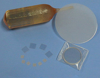
LaAlO3 substrates,10X10mm small square Lanthanum aluminate LaAlO3crystal substrate single crystals

--------------------------------------------------------------------------------------------------------------


Application:

LaAlO3 single crystal is the most important single crystal material of high temperature superconducting thin film. Growth of pulling method is CZ method, which can get 2 inches diameter and larger single crystal and the substrate, it  has high temperature superconducting material such as YBaCuO and lattice match well, low dielectric constant and microwave loss is small, which is suitable for making high temperature superconducting microwave electronic devices (such as telecommunication of HTS microwave filter, etc.)

General Properties

Product Name:Lanthanum aluminate (LaAlO3) crystal substrate
Product Description:LaAlO3 perovskite crystal structure of materials on a variety of good lattice matching is epitaxial HTS thin films and giant magnetoresistance excellent substrate material, its dielectric properties suitable for low loss microwave dielectric resonator and the application of . HB is the world's largest existing lanthanum aluminate single crystal growth of manufacturers, the monthly production of 10 to 20 kg can, can provide rods, sheets and cutting rough epitaxial substrate polishing to meet the diverse needs of the global market.
Technical parameters:
Crystal structurePseudo-cubic
Lattice constanta = 3. 792Å
Growth methodCzochralski method
Mp2080 °C
Density6.52g/cm3
Mohs hardness6.5 Mohs
Thermal expansion coefficient10 × 10 -6 / °C
Permittivity25
Loss tangent (10GHz)~ 3 × 10 -4 @ 300K, ~ 0.6 × 10 -4 @ 77K
Color and AppearanceBy annealing conditions different from brown-yellow to brown polishing a substrate with natural twinned domain
Chemical stabilityMineral acids, insoluble at room temperature, the temperature is higher than 150 °C soluble H 3 PO 4
Specifications:

<100>, <110>, <111> Tolerance: + / -0.5 degrees

dia3 "x0.5mm, dia2" x0.5mm, dia1 "x0.5mm, 10x10x0.5mm, 10x5x0.5mm

Single throw or double throw, Ra <5A

Can be customized orientation and size.

Standard Packaging:1000 clean room, 100 clean bag or single box packaging


FAQ –
Q: What you can supply logistics and cost?
(1) We accept DHL, Fedex, TNT, UPS, EMS, SF and etc.
(2) If you have your own express number, it's great.
If not, we could assist you to deliver. Freight=USD25.0(the first weight) + USD12.0/kg

Q: What's the delivery time?
(1) For the standard products such as ball lens, powell lens and collimator lens:
For inventory: the delivery is 5 workdays after order.
For customized products: the delivery is 2 or 3 workweeks after order.
(2) For the off-standard products, the delivery is 2 or 6 workweeks after you place the order.

Q: How to pay?
100%T/T, Paypal, West Union, MoneyGram, Secure payment and Trade

Assurance on Alibaba and etc..

Q: What's the MOQ?
(1) For inventory, the MOQ is 5pcs.
(2) For customized products, the MOQ is 5pcs-20pcs.
It depends on quantity and technics

Q: Do you have inspection report for material?
We can supply detail report for our products.
 

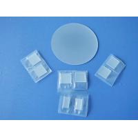
Packaging – Logistcs
Worldhawk concerns each details of the package , cleaning, anti-static , shock treatment .

According to the quantity and shape of the product , we will take a different packaging process!


Hot Products

2inch M-axis 0.5mm thickness sapphire wafer for epi-ready test ,sapphire optical windows, M-axis ...
ultrathin sapphire glass wafer ,2inch C-axis sapphire wafer for epi-ready,sapphire thick glass lens ...
ultrathin sapphire glass wafer ,2inch 0.1mm thickness sapphire wafer, 10x10x0.1mmt sapphire ...
2inch A-axis <11-20> orientation sapphire wafer for epi-ready test ,sapphire optical windows, m-axis...
Sapphire Crystal Cr3+Doped Ruby Cr Al2O3 Crystal Substrate Ruby Wafer Polishing Specification for ...
0.3mm/0.4mm/0.5mm sapphire window thin glass wafers for semiconductor or electron Optical Windows ...