
|
|
[China]

Trade Verify
Address: Rm5-616,No.851,Dianshanhu avenue, Qingpu area,Shanghai city,CHINA
Contact name:Wang

SHANGHAI FAMOUS TRADE CO.,LTD |
|
Verified Suppliers
|
|
|
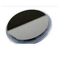
2inch GaAs substrates, GaAs wafer for led,Gallium Arsenide crystal Wafers,Si/Zn Dopant GaAs wafer(A compound of the elements gallium and arsenic. It is a III-V direct bandgap semiconductor with a zinc blende crystal structure)
--------------------------------------------------------------------------------------------------------------
Application:
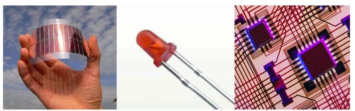
1. Mainly used in electronics, low temperature alloys, Gallium Arsenide.
2. The primary chemical compound of gallium in electronics, is used in microwave circuits, high-speed switching circuits, and infrared circuits.
3. Gallium Nitride and Indium Gallium Nitride, for semiconductor uses, produce blue and violet light-emitting diodes (LEDs) and diode lasers.
Specification
Parameter | Guaranteed / Actual Values | UOM | |
| Growth Method: | VGF | ||
| Conduct Type: | S-I-N | ||
| Dopant: | Undoped | ||
| Diameter: | 50.8± 0.1 | mm | |
| Orientation: | (100)± 0.50 | ||
| OF location/length: | EJ [ 0-1-1]± 0.50/16±1 | ||
| IF location/length: | EJ [ 0-1 1 ]± 0.50/7±1 | ||
| Resistivity: | Min: 1.0 E8 | Max: 2.2 E8 | Ω·cm |
| Mobility: | >2000 | cm2/v.s | |
| EPD: | <1500 | / cm2 | |
| Thickness: | 350± 20 | µm | |
| Edge Rounding: | 0.25 | mmR | |
| Laser Marking: | N/A | ||
| TTV/TIR: | Max: 10 | µm | |
| BOW: | Max: 10 | µm | |
| Warp: | Max: 10 | µm | |
| Partical Count: | <50/wafer(for particle>0.3um) | ||
| Surface Finish– front: | Polished | ||
| Surface Finish –back: | Etched | ||
| Epi-Ready: | Yes | ||
| Parameter | Customer’s Requirements | Guaranteed / Actual Values | UOM | ||
| Growth Method: | VGF | VGF | |||
| Conduct Type: | S-C-P | S-C-P | |||
| Dopant: | GaAs-Zn | GaAs-Zn | |||
| Diameter: | 50.8± 0.4 | 50.8± 0.4 | mm | ||
| Orientation: | (100)± 0.50 | (100)± 0.50 | |||
| OF location/length: | EJ [ 0-1-1]± 0.50/16±1 | EJ [ 0-1-1]± 0.50/16±1 | |||
| IF location/length: | EJ [ 0-1 1 ]± 0.50/7±1 | EJ [ 0-1 1 ]± 0.50/7±1 | |||
| Ingot CC: | Min: 1 E19 | Max: 5 E19 | Min: 1.4 E19 | Max: 1.9 E19 | /cm3 |
| Resistivity: | Min: N/A | Max: N/A | Min: N/A | Max: N/A | Ω·cm |
| Mobility: | Min: N/A | Max: N/A | Min: N/A | Max: N/A | cm2/v.s |
| EPD: | Max: 5000 | Min: 600 | Max: 700 | / cm2 | |
| Thickness: | 350±25 | 350±25 | µm | ||
| Surface Finish– front: | Polished | Polished | |||
| Surface Finish –back: | Etched | Etched | |||
| Epi-Ready: | Yes | Yes | |||

FAQ –
Q: What you can supply logistics and cost?
(1) We accept DHL, Fedex, TNT, UPS, EMS, SF and etc.
(2) If you have your own express number, it's great.
If not, we could assist you to deliver. Freight=USD25.0(the first
weight) + USD12.0/kg
Q: What's the delivery time?
(1) For the standard products such as ball lens, powell lens and
collimator lens:
For inventory: the delivery is 5 workdays after order.
For customized products: the delivery is 2 or 3 workweeks after
order.
(2) For the off-standard products, the delivery is 2 or 6 workweeks
after you place the order.
Q: How to pay?
T/T, Paypal, West Union, MoneyGram, Secure payment and Trade
Assurance on Alibaba and etc..
Q: What's the MOQ?
(1) For inventory, the MOQ is 5pcs.
(2) For customized products, the MOQ is 5pcs-20pcs.
It depends on quantity and technics
Q: Do you have inspection report for material?
We can supply detail report for our products.
Packaging – Logistcs
Worldhawk concerns each details of the package , cleaning,
anti-static , shock treatment .
According to the quantity and shape of the product , we will take a different packaging process!


