|
|
[China]

Trade Verify
Address: Rm5-616,No.851,Dianshanhu avenue, Qingpu area,Shanghai city,CHINA
Contact name:Wang

SHANGHAI FAMOUS TRADE CO.,LTD |
|
Verified Suppliers
|
|
|
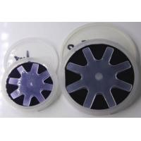
4inch Semi-Insulating Indium Phosphide InP Wafer for LD Laser Diode,semiconductor wafer,3inch InP wafer,single crystal wafer2inch 3inch 4inch InP substrates for LD application, semiconductor wafer,InP wafer,single crystal wafer
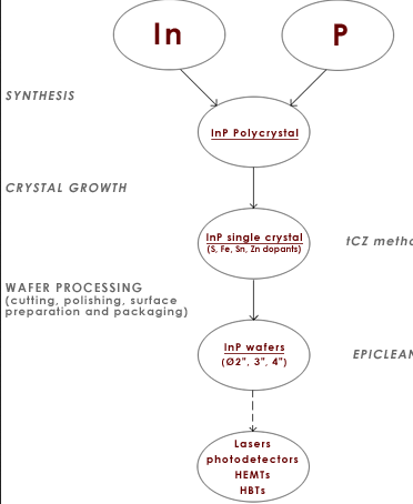
InP introduce
| InP single crystal | |
growth (modified Czochralski method) is used to pull a single crystal through a boric oxide liquid encapsulant starting from a seed. The dopant (Fe, S, Sn or Zn)is added to the crucible along with the
polycrystal. High pressure is applied inside the chamber to prevent
decomposition of the Indium Phosphide.he company has developed a process to yield fully stoechiometric, high
purity and low dislocation density inP single crystal. to a thermal baffle technology in connection with a numerical modeling of thermal growth conditions. tCZ is a cost-effective mature technology with high quality reproducibility from boule to boule | |
Specification
Fe Doped InP
Semi-Insulating InP Specifications
| Growth Method | VGF |
| Dopant | Iron (FE) |
| Wafer Shape | Round (DIA: 2", 3", AND 4") |
| Surface Orientation | (100)±0.5° |
*Other Orientations maybe available upon request
| Resistivity (Ω.cm) | ≥0.5 × 10⁷ |
| Mobility (cm2/V.S) | ≥ 1,000 |
| Etch Pitch Density (cm2) | 1,500-5,000 |
| Wafer Diameter (mm) | 50.8±0.3 | 76.2±0.3 | 100±0.3 |
| Thickness (µm) | 350±25 | 625±25 | 625±25 |
| TTV [P/P] (µm) | ≤ 10 | ≤ 10 | ≤ 10 |
| TTV [P/E] (µm) | ≤ 10 | ≤ 15 | ≤ 15 |
| WARP (µm) | ≤ 15 | ≤ 15 | ≤ 15 |
| OF (mm) | 17±1 | 22±1 | 32.5±1 |
| OF / IF (mm) | 7±1 | 12±1 | 18±1 |
| Polish* | E/E, P/E, P/P | E/E, P/E, P/P | E/E, P/E, P/P |
*E=Etched, P=Polished
Note: Other Specifications maybe available upon request
n- and p-type InP
Semi-conducting InP Specifications
| Growth Method | VGF |
| Dopant | n-type: S, Sn AND Undoped; p-type: Zn |
| Wafer Shape | Round (DIA: 2", 3", AND 4") |
| Surface Orientation | (100)±0.5° |
*Other Orientations maybe available upon request
| Dopant | S & Sn (n-type) | Undoped (n-type) | Zn (p-type) |
| Carrier Concentration (cm-3) | (0.8-8) × 1018 | (1-10) × 1015 | (0.8-8) ×1018 |
| Mobility (cm2/V.S.) | (1-2.5) × 103 | (3-5) × 103 | 50-100 |
| Etch Pitch Density (cm2) | 100-5,000 | ≤ 5000 | ≤ 500 |
| Wafer Diameter (mm) | 50.8±0.3 | 76.2±0.3 | 100±0.3 |
| Thickness (µm) | 350±25 | 625±25 | 625±25 |
| TTV [P/P] (µm) | ≤ 10 | ≤ 10 | ≤ 10 |
| TTV [P/E] (µm) | ≤ 10 | ≤ 15 | ≤ 15 |
| WARP (µm) | ≤ 15 | ≤ 15 | ≤ 15 |
| OF (mm) | 17±1 | 22±1 | 32.5±1 |
| OF / IF (mm) | 7±1 | 12±1 | 18±1 |
| Polish* | E/E, P/E, P/P | E/E, P/E, P/P | E/E, P/E, P/P |
*E=Etched, P=Polished
Note: Other Specifications maybe available upon request
| InP Wafer processing | |
| Each ingot is cut into wafers which are lapped, polished and surface prepared for epitaxy. The overall process is detailed hereunder. | |
| Flat specification and identification | The orientation is indicated on the wafers by two flats (long flat for orientation, small flat for identification). Usually the E.J. standard (European-Japanese) is used. The alternate flat configuration (U.S.) is mostly used for Ø 4" wafers. |
| Orientation of the boule | Either exact (100) or misoriented wafers are offered. |
| Accuracy of the orientation of OF | In response to the needs of the optoelectronic industry, we offers wafers with excellent accuracy of the OF orientation : < 0.02 degrees. This feature is an important benefit to customers making edge-emitting lasers and also to manufacturers who cleave to separate dies allowing their designers to reduce the real-estate wasted in the streets. |
| Edge profile | There are two common specs : chemical edge processing or mechanical edge processing (with an edge grinder). |
| Polishing | Wafers are polished by means of a chemical-mechanical process resulting in a flat, damage-free surface. we provides both double-side polished and single-side polished (with lapped and etched back side) wafers. |
| Final surface preparation and packaging | Wafers go through many chemical steps to remove the oxide produced
during polishing and to create a clean surface with stable and
uniform oxide layer that is ready for epitaxial growth - epiready
surface and that reduces trace elements to extremely low levels .
After final inspection, the wafers are packaged in a way that
maintains the surface cleanliness. Specific instructions for oxide removal are available for all types of epitaxial technologies (MOCVD, MBE). |
| Database | As part of our Statistical Process Control/Total Quality Management Program, extensive database recording the electrical and mechanical properties for every ingot as well as crystal quality and surface analysis of wafers are available. At each stage of fabrication, the product is inspected before passing to the next stage to maintain a high level of quality consistency from wafer to wafer and from boule to boule. |


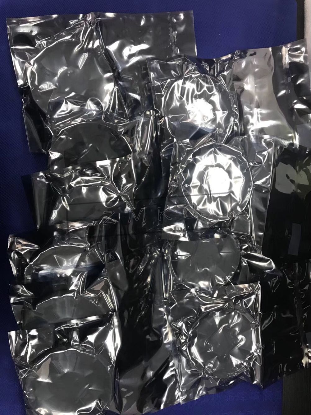
Package & delivery


FAQ:
Q: What's your MOQ and delivery time?
A: (1) For inventory, the MOQ is 5 pcs.
(2) For customized products, the MOQ is 10-30 pcs up.
(3) For customized products,the delivery time in 10days, custiomzed size for 2-3weeks