
|
|
[China]

Trade Verify
Address: Rm5-616,No.851,Dianshanhu avenue, Qingpu area,Shanghai city,CHINA
Contact name:Wang

SHANGHAI FAMOUS TRADE CO.,LTD |
|
Verified Suppliers
|

|
|
n-type 2inch prime sillicon wafer, sillicon optical lens, IC sillicon substrates , poly sillicon wafer,Semiconductor 3' inch silicon wafer, single crystal ,2inch, 3inch,4inch,5inch,6inch,8inch,12inch silicon wafer, single side polished silicon wafer
1. Description
Si is most widely used for lenses and windows in IR systems
operating in the 2 - 12 µm range. The enviroment does not make any
problems because Germanium is inert, mechanically rugged, and
fairly hard. It is an excellent choice for multi-spectral systems
and for applications where EMI shielding is necessary. Germanium
can be electrically heated for anti-fogging or anti-icing
applications. We do not manufacture Germanium, but hold stock of
Czochralsky grown material of various diameters. It can be used as
a polycrystalline or as a single crystal. The purity should
correspond to an electrical resistivity of at least 20 to 30
Ohm/cm, either p- or n-type to avoid absorption bands. The high
retractive index makes AR-coating essential.
Silicon (Si) is commonly used as a substrate material for infrared reflectors
and windows in the 1.5 - 8 µm region. The strong absorption band at
9 µm makes it unsuitable for CO2-laser transmission applications, but it is frequently used for
laser mirrors because of its high thermal conductivity and low
density. Silicon is also a usefull transmitter in the 20 µm range.
Density | 2.4(g/cm3) | ||
| Dope type | no dope | doped B | doped P |
| Type | I | P | N |
| resistivity | Ø 1000Ωcm | 10-3~40Ωcm | 10-3~40Ωcm |
| E P D | ≤100∕cm2 | ≤100∕cm2 | ≤100∕cm2 |
| Oxygen content (∕cm3) | ≤1~1.8×10¹⁸ | ≤1~1.8×10¹⁸ | ≤1~1.8×10¹⁸ |
| Carbon content(∕cm3) | ≤5×10¹⁶ | ≤5×10¹⁶ | ≤5×10¹⁶ |
| Size | 10×3m,10×5m,10×10mm,15×15mm, | ||
| Dia50.8mm,Dia76.2mm,Dia100mm | dia6-12inch | ||
| or by customized size | |||
| thickness | 0.5mm,1.0mm or other | ||
| tolerance | <±0.1mm | ||
| thickness tolerance | <±0.015mm (or <±0.005mm) | ||
| surface | 1sp or 2sp | ||
| orientation | ±0.5° | ||
| orientation | <100>,<110>,<111> | ||
| package | 100grade in1000 grade cleaning room |
2. Specification 2 Inch Silicon Wafers
Product Name | Silicon Wafer 2 inch |
Diameter | 50.8+/-0.3mm |
Thickness | 279+/-25um/Customized |
Conductivity Type | N/P |
Resistivity | Customized |
Growth Method | CZ/FZ |
Orientation | 100/111 |
Surface | Single side polished/Double side polished/ Grinding |
TTV | <10 um |
Bow/Warp | < 30 um |
Carbon Content | 18 ppma |
Oxygen Content | 1ppma |
Particles | <50 @ 0.3um |
Grade | Test Grade |


3 About our company
ZMKJ locates in the city of Shanghai, Which is the best city of China,and our factory is founded
in Wuxi city in 2014.
We specialize in processing a varity of materials
into wafers, substrates and custiomized
optical glass parts.components widely used in electronics, optics, optoelectronics and many
other fields. We also have been working closely with many domestic and oversea universities,
research institutions and companies, provide customized products and services for their R&D
projects.It's our vision to maintaining a good relationship of cooperation with our all customers
by our good reputatiaon.

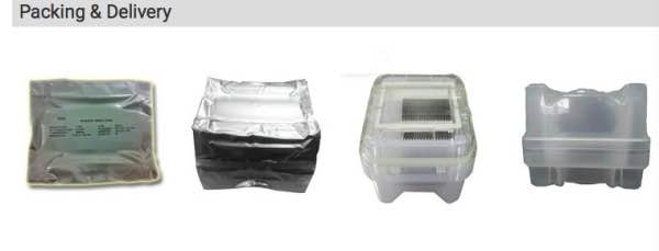
4. packing and delivery
-FAQ –
Q: What you can supply logistics and cost?
(1) We accept DHL, Fedex, TNT, UPS, EMS, SF and etc.
(2) If you have your own express number, it's great.
If not, we could assist you to deliver. Freight=USD25.0(the first
weight) + USD12.0/kg
Q: What's the delivery time?
(1) For the standard products such as ball lens, powell lens and
collimator lens:
For inventory: the delivery is 5 workdays after order.
For customized products: the delivery is 2 or 3 workweeks after
order.
(2) For the off-standard products, the delivery is 2 or 6 workweeks
after you place the order.
Q: How to pay?
50% deposit,T/T, Paypal, West Union, MoneyGram, Secure payment and
Trade Assurance
on Alibaba and etc..
Q: What's the MOQ?
(1) For inventory, the MOQ is 10pcs.
(2) For customized products, the MOQ is 10pcs-25pcs.
It depends on quantity and technics
Q: Do you have inspection report for material?
We can supply ROHS report and reach reports for our products.


