Home Companies SHANGHAI FAMOUS TRADE CO.,LTD

Al2O3 Ceramic Substrate Wafer Excellent Electrical Properties For Mechanical Seals

SHANGHAI FAMOUS TRADE CO.,LTD

Contact Us

[China] country

Trade Verify

Address: Rm5-616,No.851,Dianshanhu avenue, Qingpu area,Shanghai city,CHINA

Contact name:Wang

Inquir Now

SHANGHAI FAMOUS TRADE CO.,LTD

Verified Suppliers
  • Trust
    Seal
  • Verified
    Supplier
  • Credit
    Check
  • Capability
    Assessment

Al2O3 Ceramic Substrate Wafer Excellent Electrical Properties For Mechanical Seals

Country/Region china
City & Province shanghai shanghai
Categories Steel Sheets
InquireNow

Product Details

1.0mm Thickness Aluminum  Al2O3 Ceramic Substrate wafer, High Thermal Conductivity Al2O3 Ceramic plate ,4inch ceramic substrates wafer
 
Al2O3 Introduce

Alumina Ceramicis the most mature of the engineering ceramics, offering excellent electrical insulation properties together with high hardness and good wear resistance,but relatively low strength and fracture toughness.Alumina ceramic is generally white but may also be pink or ivory.The color is derived from either the sintering additives or impurities in the raw materials.

.STA High alumina ceramic wafer 99.7% Al2O3, Access to the list of our standard dimensions (Alumina and Zirconia Oxide) for electrical, vacuum or temperature resistance application.
 
Basic properties of high alumina ceramic wafer.
Very hard
Abrasion resistant
Can be milled with great precision
Can be polished
Stable at high temperatures
No open porosity
Excellent electrical properties
Chemically inert
High corrosion resistant
 
Applications of ceramic parts components.
Mechanical components
Pistons, pump stages
Mechanical seals
Sealing bushes
Faucet keys and seats
Electrical insulator
Pyrometry
Laboratory items, crucibles
Vacuum items
Welding nozzles


Al2O3 Ceramic Feature & Advantagement

- Product Name:Alumina / Al2O3 Ceramic Substrate For Thick Film Circuit / 5.5''x7.5''
- Material:96% Alumina
- Typical Characteristics:

1. Excellent Electrical Insulation
2. Good Thermal Shock Resistance
3. Corrosion Resistance
4. Good Flatness

- Typical Applications:

1. Thick Film Hybrid Integrated Circuit
2. Ceramic Radiating Base for LED
3. Power Module
4. Semiconductor Device

 
Regular Size
Thickness(mm)                                       lengthx width ( mm)
0.385

 
       2″* 2″
50.8mm*50.8mm


          3″* 3″
76.2mm*76.2mm
 

            4″* 4″
101.6mm*101.6mm

              4.5″* 4.5″
    114.3mm*114.3mm

0.5
0.635
1.0
                                           diameter(mm)
1.0

Φ16
Φ19

Φ20
Φ26

Φ30
Φ35

Φ40
Φ45

Φ50
Φ52

Φ60Φ75Φ80
1.2
1.5
2.0
2.5


Polishing  Service
   Our AlN substrate can be polished(single and double polish) by the advanced machine which imported
from abroad. Ceramic substrate surface roughness can reach to 1nm without porous after being polished.
  It is perfectly suitable for the device application of small spec, high precision , wiring density and good stability.

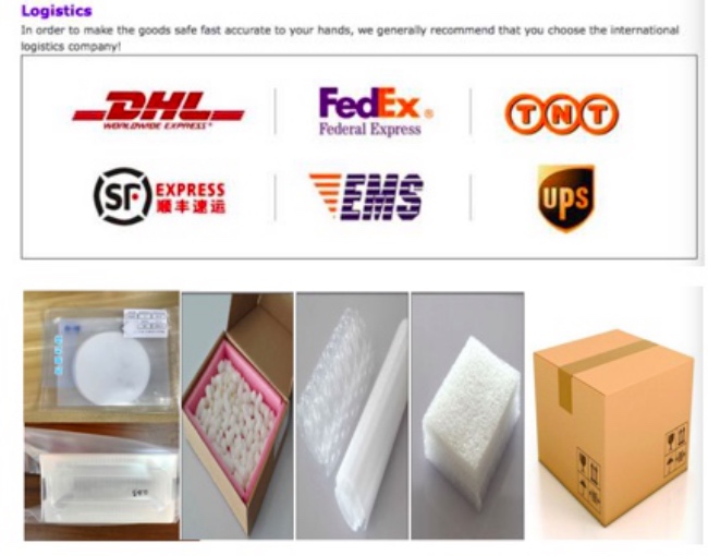
Package & Delivery


Hot Products

2inch M-axis 0.5mm thickness sapphire wafer for epi-ready test ,sapphire optical windows, M-axis ...
ultrathin sapphire glass wafer ,2inch C-axis sapphire wafer for epi-ready,sapphire thick glass lens ...
ultrathin sapphire glass wafer ,2inch 0.1mm thickness sapphire wafer, 10x10x0.1mmt sapphire ...
2inch A-axis <11-20> orientation sapphire wafer for epi-ready test ,sapphire optical windows, m-axis...
Sapphire Crystal Cr3+Doped Ruby Cr Al2O3 Crystal Substrate Ruby Wafer Polishing Specification for ...
0.3mm/0.4mm/0.5mm sapphire window thin glass wafers for semiconductor or electron Optical Windows ...