|
|
[China]

Trade Verify
Address: Building 11, Lane 1333, Jiangnan Avenue, Changxing Town, Chongming District, Shanghai
Contact name:Xiwen Bai (Ciel)

Shanghai GaNova Electronic Information Co., Ltd. |
|
Verified Suppliers
|

|
|
4 inch N-type Si-doped GaN on sapphire wafer SSP resistivity<0.05 Ω cm LED, laser, PIN epitaxial wafer
For lightly Si-doped GaN ([Si] = 2.1 × 1016 cm−3), the room temperature (RT) electron mobility was as high as 1008 cm2 V−1 s−1, which was dominantly limited by polar optical phonon scattering. Moreover, we found that heavily Si-doped GaN prepared using PSD exhibited an RT mobility as high as 110 cm2 V−1 s−1 at an electron concentration of 2 × 1020 cm−3, which indicated that the resistivity of this film was almost as small as those of typical transparent conductive oxides such as indium tin oxide.
At lower temperatures, the electron mobility increased to 1920 cm2 V−1 s−1 at 136 K, and the temperature dependence was well explained by conventional scattering models. These results indicate that Si-doped GaN prepared using PSD is promising not only for the fabrication of GaN-based power devices but also for use as epitaxial transparent electrode materials for nitride based optical devices.
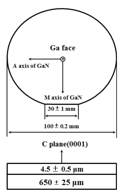
| 4-inch Si-doped GaN/Sapphire Substrates | ||
| Item | GaN-T-C-N-C100 |
|
| Dimensions | 100 ± 0.2 mm | |
| Thickness/Thickness STD | 4.5 ± 0.5 μm / < 3% | |
| Orientation | C plane (0001) off angle toward A-axis 0.2 ± 0.1 ° | |
| Orientation Flat of GaN | (1-100) 0 ± 0.2 °, 30 ± 1 mm | |
| Conduction Type | N-type | |
| Resistivity (300K) | < 0.05 Ω·cm | |
| Carrier Concentration | > 1 x 1018 cm-3( ≈ doping concentration) | |
| Mobility | > 200 cm2/V·s | |
| *XRD FWHMs | (0002) < 300 arcsec,(10-12) < 400 arcsec | |
| Structure | ~ 2μm nGaN /~ 2.5μm uGaN /~ 25 nm uGaN buffer/650 ± 25 μm sapphire | |
| Orientation of Sapphire | C plane (0001) off angle toward M-axis 0.2 ± 0.1 ° | |
| Orientation Flat of Sapphire | (11-20) 0 ± 0.2 °, 30 ± 1 mm | |
| Sapphire Polish | Single side polished (SSP) / Double side polished (DSP) | |
| Useable Area | > 90% (edge and macro defects exclusion) | |
| Package | Packaged in a cleanroom in containers: single wafer box (< 3 PCS) or cassette (≥ 3 PCS) | |
About Us
We specialize in processing a variety of materials into wafers, substrates and customized optical glass parts.components widely used in electronics, optics, opto electronics and many other fields. We also have been working closely with many domestic and oversea universities, research institutions and companies, provide customized products and services for their R&D projects. It's our vision to maintaining a good relationship of cooperation with our all customers by our good reputations.
FAQ
Q: Are you trading company or manufacturer ?
We are factory.
Q: How long is your delivery time?
Generally it is 3-5 days if the goods are in stock.
or it is 7-10 days if the goods are not in stock, it is according
to quantity.
Q: Do you provide samples ? is it free or extra ?
Yes, we could offer the sample for free charge but do not pay the
cost of freight.
Q: What is your terms of payment ?
Payment <=5000USD, 100% in advance.
Paymen >=5000USD, 80% T/T in advance , balance before shippment.