
|
|
[China]

Trade Verify
Address: Building 11, Lane 1333, Jiangnan Avenue, Changxing Town, Chongming District, Shanghai
Contact name:Xiwen Bai (Ciel)

Shanghai GaNova Electronic Information Co., Ltd. |
|
Verified Suppliers
|
|
|
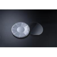
Dimension 100 ± 0.2mm 4 Inch Blue LED GaN Epitaxial Wafer On Sapphire SSP Thickness 5.5 ± 0.5μm
4 inch Blue LED GaN epitaxial wafer on sapphire SSP
Researchers from North Carolina State University and Purdue
University have shown that the semiconductor material gallium
nitride (GaN) is non-toxic and is compatible with human cells –
opening the door to the material's use in a variety of biomedical
implant technologies.
LEDs, light emitting diodes, are light sources that are energy
efficient and can be made in a variety of colors. Gallium is a main
component in many LED lights, with different gallium compounds
producing different colored light when exposed to an electric
current.
| 4inch GaN-on-Sapphire Blue/Green LED Wafer | ||||
Substrate | Type | Flat Sapphire |
| |
| Polish | Single side polished (SSP) / Double side polished (DSP) | |||
| Dimension | 100 ± 0.2 mm | |||
| Orientation | C plane (0001) off angle toward M-axis 0.2 ± 0.1° | |||
| Thickness | 650 ± 25 μm | |||
Epilayer | Structure | 0.2μm pGaN/0.5μm MQWs/2.5μm nGaN/2.0μm uGaN | ||
| Thickness | 5.5 ± 0.5μm | |||
| Roughness (Ra) | <0.5 nm | |||
| Dislocation density | < 5 × 108 cm-2 | |||
| Wavelength | Blue LED | Green LED | ||
| 465 ± 10 nm | 525 ± 10 nm | |||
| Wavelength FWHMs | < 25 nm | < 40 nm | ||
| Chip Performance | Cut-in voltage@1μA | 2.3-2.5V | 2.2-2.4V | |
| Useable Area | > 90% (edge and macro defects exclusion) | |||
Package |
Packaged in a cleanroom in a single wafer container | |||
About Us
We specialize in processing a variety of materials into wafers, substrates and customized optical glass parts.components widely used in electronics, optics, opto electronics and many other fields. We also have been working closely with many domestic and oversea universities, research institutions and companies, provide customized products and services for their R&D projects. It's our vision to maintaining a good relationship of cooperation with our all customers by our good reputations.
FAQ
Q: Are you trading company or manufacturer ?
We are factory.
Q: How long is your delivery time?
Generally it is 3-5 days if the goods are in stock.
or it is 7-10 days if the goods are not in stock, it is according
to quantity.
Q: Do you provide samples ? is it free or extra ?
Yes, we could offer the sample for free charge but do not pay the
cost of freight.
Q: What is your terms of payment ?
Payment <=5000USD, 100% in advance.
Paymen >=5000USD, 80% T/T in advance , balance before shippment.


