
|
|
[China]

Trade Verify
Address: Building 11, Lane 1333, Jiangnan Avenue, Changxing Town, Chongming District, Shanghai
Contact name:Xiwen Bai (Ciel)

Shanghai GaNova Electronic Information Co., Ltd. |
|
Verified Suppliers
|
|
|
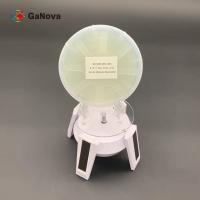
JDCD03-001-003
Overview
A SiC wafer is a semiconductor material that has excellent
electrical and thermal properties. It is a high-performance
semiconductor that is ideal for a wide variety of applications. In
addition to its high thermal resistance, it also features a very
high level of hardness.
Property | P-MOS Grade | P-SBD Grade | D Grade |
| Crystal Form | 4H | ||
| Polytype | None Permitted | Area≤5% | |
| (MPD) a | ≤0.2 /cm2 | ≤0.5 /cm2 | ≤5 /cm2 |
| Hex Plates | None Permitted | Area≤5% | |
| Hexagonal Polycrystal | None Permitted | ||
| Inclusions a | Area≤0.05% | Area≤0.05% | N/A |
| Resistivity | 0.015Ω•cm—0.025Ω•cm | 0.015Ω•cm—0.025Ω•cm | 0.014Ω•cm—0.028Ω•cm |
| (EPD)a | ≤4000/cm2 | ≤8000/cm2 | N/A |
| (TED)a | ≤3000/cm2 | ≤6000/cm2 | N/A |
| (BPD)a | ≤1000/cm2 | ≤2000/cm2 | N/A |
| (TSD)a | ≤600/cm2 | ≤1000/cm2 | N/A |
| Stacking Fault | ≤0.5% Area | ≤1% Area | N/A |
Surface Metal Contamination |
(Al, Cr, Fe, Ni, Cu, Zn, Pb, Na, K, Ti, Ca ,V, Mn) ≤1E11 cm-2 | ||
| Diameter | 150.0 mm +0mm/-0.2mm | ||
| Surface Orientation | Off-Axis:4°toward <11-20>±0.5 ° | ||
| Primary Flat Length | 47.5 mm ± 1.5 mm | ||
| Secondary Flat Length | No Secondary Flat | ||
| Primary Flat Orientation | Parallel to<11-20>±1° | ||
| Secondary Flat Orientation | N/A | ||
| Orthogonal Misorientation | ±5.0° | ||
| Surface Finish | C-Face:Optical Polish,Si-Face:CMP | ||
| Wafer Edge | Beveling | ||
Surface Roughness (10μm×10μm) | Si Face Ra≤0.20 nm ; C Face Ra≤0.50 nm | ||
| Thickness a | 350.0μm± 25.0 μm | ||
| LTV(10mm×10mm)a | ≤2μm | ≤3μm | |
| (TTV)a | ≤6μm | ≤10μm | |
| (BOW) a | ≤15μm | ≤25μm | ≤40μm |
| (Warp) a | ≤25μm | ≤40μm | ≤60μm |
| Chips/Indents | None Permitted ≥0.5mm Width and Depth | Qty.2 ≤1.0 mm Width and Depth | |
Scratches a (Si Face,CS8520) | ≤5 and Cumulative Length≤0.5×Wafer Diameter | ≤5 and Cumulative Length≤1.5×Wafer Diameter | |
| TUA(2mm*2mm) | ≥98% | ≥95% | N/A |
| Cracks | None Permitted | ||
| Contamination | None Permitted | ||
| Property | P-MOS Grade | P-SBD Grade | D Grade |
| Edge Exclusion | 3mm | ||
Remark: 3mm edge exclusion is used for the items marked with a.
About Us
We specialize in processing a variety of materials into wafers, substrates and customized optical glass parts.components widely used in electronics, optics, opto electronics and many other fields. We also have been working closely with many domestic and oversea universities, research institutions and companies, provide customized products and services for their R&D projects. It's our vision to maintaining a good relationship of cooperation with our all customers by our good reputations.
FAQ
Q: Are you trading company or manufacturer ?
We are factory.
Q: How long is your delivery time?
Generally it is 3-5 days if the goods are in stock.
or it is 7-10 days if the goods are not in stock, it is according
to quantity.
Q: Do you provide samples ? is it free or extra ?
Yes, we could offer the sample for free charge but do not pay the
cost of freight.
Q: What is your terms of payment ?
Payment <=5000USD, 100% in advance.
Paymen >=5000USD, 80% T/T in advance , balance before shippment.


