|
|
[China]

Trade Verify
Address: West of 2nd Floor, Building 10, Zhengzhong Science Park, Xintian Community, Fuhai Street, Bao'an District, Shenzhen China 518103
Contact name:Yoyo

Shenzhen Huafu Fast Multilayer Circuit Co. LTD |
|
Verified Suppliers
|
|
|
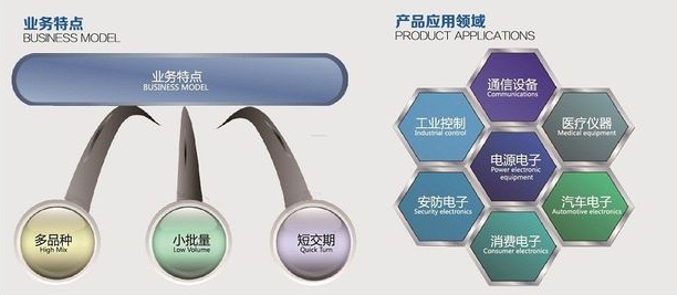
Application
Products are applied to a wide range of High-tech industries such
as: LED, telecommunication, computer application, lighting, game
machine, industrial control, power, automobile and high-end
consumer electronics, ect. By unremitting work and effort to the
marketing, products exports to American, Canada, Europe counties,
Africa and other Asia-pacific countries
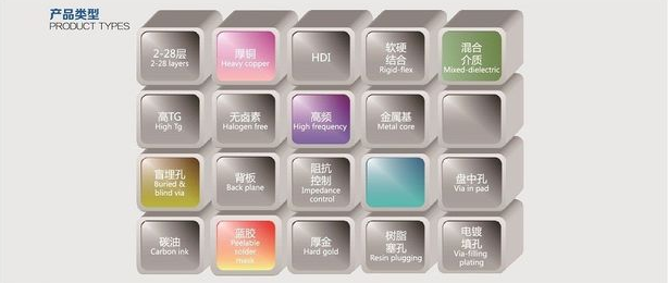
Capability
| High precision prototype | PCB bulk production | ||
| Max Layers | 1-28 layers | 1-14 layers | |
| MIN Line width(mil) | 3mil | 4mil | |
| MIN Line space(mil) | 3mil | 4mil | |
| Min via (mechanical drilling) | Board thickness≤1.2mm | 0.15mm | 0.2mm |
| Board thickness≤2.5mm | 0.2mm | 0.3mm | |
| Board thickness>2.5mm | Aspect Ration≤13:1 | Aspect Ration≤13:1 | |
| Aspect Ration | Aspect Ration≤13:1 | Aspect Ration≤13:1 | |
| Board thickness | MAX | 8mm | 7mm |
| MIN | 2 layers:0.2mm;4 layers:0.35mm;6 layers:0.55mm;8 layers:0.7mm;10 layers:0.9mm | 2 layers:0.2mm;4 layers:0.4mm;6 layers:0.6mm;8layers:0.8mm | |
| MAX Board size | 610*1200mm | 610*1200mm | |
| Max copper thickness | 0.5-6oz | 0.5-6oz | |
| Immersion Gold/ Gold Plated Thickness | Immersion Gold:Au,1—8u” Gold finger:Au,1—150u” Gold Plated:Au,1—150u” Nickel Plated :50—500u” | ||
| Hole copper thick | 25um 1mil | 25um 1mil | |
| Tolerance | Board thickness | Board thickness≤1.0mm:+/-0.1mm 1.0mm<Board thickness≤2.0mm:+/-10% Board thickness>2.0mm:+/-8% | Board thickness≤1.0mm:+/-0.1mm 1.0mm<Board thickness≤2.0mm:+/-10% Board thickness>2.0mm:+/-8% |
| Outline Tolerance | ≤100mm:+/-0.1mm 100< ≤300mm:+/-0.15mm >300mm:+/-0.2mm | ≤100mm:+/-0.13mm 100< ≤300mm:+/-0.15mm >300mm:+/-0.2mm | |
| Impedance | ±10% | ±10% | |
| MIN Solder mask bridge | 0.08mm | 0.10mm | |
| Plugging Vias capability | 0.25mm--0.60mm | 0.70mm--1.00mm | |
Advantages
1. PCB factory directly
2. Comprehensive quality control system
3. Competitive price
4. Quick turn delivery time from 48hours.
5. Certificates (ISO/UL E354810/RoHS)
6. 9 years experience in exporting service
7. No MOQ/MOV.
8. High quality. Strict through the AOI(Automated Optical
Inspection), QA/QC, flying porbe ,Etesting, etc