

Active Member
|
[China]

Address: Room 36B1-B2, Building C, Electronics Science & Technology Building Shennan Mid-Road, Shenzhen China
Contact name:Sharon Yang

Anterwell Technology Ltd. |

|
|
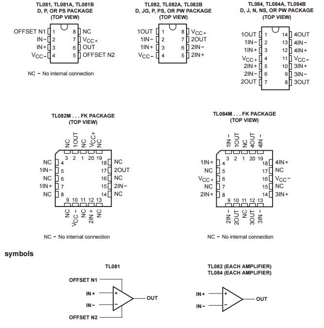
TL081, TL081A, TL081B, TL082, TL082A, TL082B,
TL084, TL084A, TL084B
JEET-INPUT OPERTIONAL AMPLIFERS
description/ordering information
The TL08x JFET-input operational amplifier family is designed to offer a wider selection than any previously developed operational amplifier family. Each of these JFET-input operational amplifiers incorporates well-matched, high-voltage JFET and bipolar transistors in a monolithic integrated circuit. The devices feature high slew rates, low input bias and offset currents, and low offset-voltage temperature coefficient. Offset adjustment and external compensation options are available within the TL08x family.
The C-suffix devices are characterized for operation from 0°C to 70°C. The I-suffix devices are characterized for operation from −40°C to 85°C. The Q-suffix devices are characterized for operation from −40°C to 125°C. The M-suffix devices are characterized for operation over the full military temperature range of −55°C to 125°C.
absolute maximum ratings over operating free-air temperature range
(unless otherwise noted)†
TL08_C TL08_AC TL08_BC | TL08_I | TL084Q | TL08_M | UNIT | ||
| Supply voltage, VCC+ (see Note 1) | 18 | V | ||||
| Supply voltage VCC− (see Note 1) | -18 | V | ||||
| Differential input voltage, VID (see Note 2) | ± 30 | V | ||||
| Input voltage, VI (see Notes 1 and 3) | ± 15 | V | ||||
| Duration of output short circuit (see Note 4) | Unlimited | |||||
| Continuous total power dissipation | See Dissipation Rating Table | |||||
| Operating free-air temperature range, TA | 0 to 70 | − 40 to 85 | − 40 to 125 | − 55 to 125 | °C | |
| Package thermal impedance, θJA (see Notes 5 and 6) | D package (8-pin) | 97 | 97 | °C/W | ||
| D package (14-pin) | 86 | 86 | ||||
| N package (14-pin) | 76 | 76 | ||||
| NS package (14-pin) | 80 | |||||
| P package (8-pin) | 85 | 85 | ||||
| PS package (8-pin) | 95 | 95 | ||||
| PW package (8-pin) | 149 | |||||
| PW package (14-pin) | 113 | 113 | ||||
| Operating virtual junction temperature | 150 | °C | ||||
| Case temperature for 60 seconds, TC | FK package | 260 | °C | |||
| Lead temperature 1,6 mm (1/16 inch) from case for 60 seconds | J or JG package | 300 | °C | |||
| Storage temperature range, Tstg | − 65 to 150 | °C | ||||
† Stresses beyond those listed under “absolute maximum ratings” may cause permanent damage to the device. These are stress ratings only, and functional operation of the device at these or any other conditions beyond those indicated under “recommended operating conditions” is not implied. Exposure to absolute-maximum-rated conditions for extended periods may affect device reliability.
NOTES:
1. All voltage values, except differential voltages, are with respect to the midpoint between VCC+ and VCC−.
2. Differential voltages are at IN+ with respect to IN−.
3. The magnitude of the input voltage must never exceed the magnitude of the supply voltage or 15 V, whichever is less.
4. The output may be shorted to ground or to either supply. Temperature and/or supply voltages must be limited to ensure that the dissipation rating is not exceeded.
5. Maximum power dissipation is a function of TJ(max), θJA, and TA. The maximum allowable power dissipation at any allowable ambient temperature is PD = (TJ(max) − TA)/θJA. Operating at the absolute maximum TJ of 150°C can affect reliability.
6. The package thermal impedance is calculated in accordance with JESD 51-7.
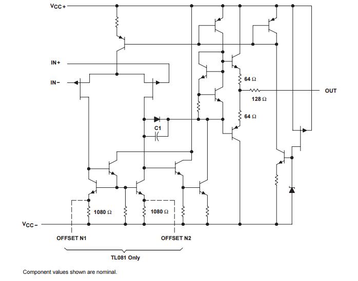
schematic (each amplifier)
Stock Offer (Hot Sell)
| Part NO. | Q'ty | MFG | D/C | Package |
| MC100LVELT23DR2G | 2265 | ON | 16+ | SOP |
| MPXV5004DP | 4162 | FREESCALE | 14+ | SOP |
| MAX3430CSA+ | 12550 | MAXIM | 16+ | SOP |
| LTC1060CN | 14790 | LT | 14+ | DIP |
| 53398-0371 | 10000 | MOLEX | 15+ | connector |
| 53398-0571 | 5071 | MOLEX | 15+ | connector |
| NDB6020P | 10000 | FAIRCHILD | 10+ | TO-263 |
| MBR1645G | 15910 | ON | 15+ | TO-220 |
| MMSZ6V8T1G | 25000 | ON | 16+ | SOD-123 |
| LP2975AIMM-3.3 | 3855 | NSC | 15+ | MSOP-8 |
| BZX84C15LT1G | 10000 | ON | 15+ | SOT-23 |
| PIC16F916-I/SO | 4738 | MICROCHIP | 16+ | SOP |
| PCF8593T | 13300 | NXP | 16+ | SOP |
| MSP430F2481TPMR | 6736 | TI | 16+ | LQFP |
| ZXMN2A03E6TA | 9000 | ZETEX | 15+ | SOT23-6 |
| NTD5865NLT4G | 4580 | ON | 16+ | TO-252 |
| P89LPC915FDH | 10240 | NXP | 16+ | TSSOP |
| LP339MX | 6675 | NSC | 14+ | SOP-14 |
| MMBFJ309LT1G | 10000 | ON | 16+ | SOT-23 |
| MBRM360-13-F | 17923 | DIODES | 16+ | SDT |
| MC68HC908QY4ACPE | 3826 | FREESCALE | 14+ | DIP |


