

Active Member
|
[China]

Address: Room 36B1-B2, Building C, Electronics Science & Technology Building Shennan Mid-Road, Shenzhen China
Contact name:Sharon Yang

Anterwell Technology Ltd. |
|
|
DABiC-IV, 10-BIT SERIAL-INPUT, LATCHED SOURCE DRIVERS
The A6809– and A6810– devices combine 10-bit CMOS shift registers, accompanying data latches and control circuitry with bipolar sourcing outputs and pnp active pull downs. Designed primarily to drive vacuum-fluorescent displays, the 60 V and -40 mA output ratings also allow these devices to be used in many other peripheral power driver applications. The A6809– and A6810– feature an increased data input rate (compared with the older UCN/UCQ5810-F) and a controlled output slew rate. The A6809xLW and A6810xLW are identical except for pinout.
The CMOS shift register and latches allow direct interfacing with microprocessor-based systems. With a 3.3 V or 5 V logic supply, typical serial-data input rates are up to 33 MHz.
A CMOS serial data output permits cascade connections in applications requiring additional drive lines. Similar devices are avail-able as the A6811– (12 bits), A6812– (20 bits), and A6818– (32 bits).
The A6809– and A6810– output source drivers are npn Darlingtons, capable of sourcing up to 40 mA. The controlled output slew rate reduces electromagnetic noise, which is an important consideration in systems that include telecommunications and/or microprocessors and to meet government emissions regulations. For inter-digit blanking, all output drivers can be disabled and all sink drivers turned on with a BLANKING input high. The pnp active pull-downs will sink at least 2.5 mA.
All devices are available in two temperature ranges for optimum performance in commercial (suffix S-) or industrial (suffix E-) applications. The A6810– is provided in three package styles for through-hole DIP (suffix -A), surface-mount SOIC (suffix -LW), or minimum-area surface-mount PLCC (suffix -EP). The A6809– is provided in the SOIC (suffix -LW) only. Copper lead frames, low logic-power dissipation, and low output-saturation voltages allow all devices to source 25 mA from all outputs continuously over the maximum operating temperature range.
FEATURES
■ Controlled Output Slew Rate
■ High-Speed Data Storage
■ 60 V Minimum Output Breakdown
■ High Data Input Rate
■ PNP Active Pull-Downs
■ Low Output-Saturation Voltages
■ Low-Power CMOS Logic and Latches
■ Improved Replacements for TL4810–, UCN5810–, and UCQ5810–
ABSOLUTE MAXIMUM RATINGS at TA = 25°C
Logic Supply Voltage, VDD ................................................................................... 7.0 V
Driver Supply Voltage, VBB ................................................................................... 60 V
Continuous Output Current Range, IOUT .......................................... -40 mA to +15 mA
Input Voltage Range, VIN ............................................................ -0.3 V to VDD + 0.3 V
Package Power Dissipation, PD .................................................................... See Graph
Operating Temperature Range, TA (Suffix ‘E–’) ...................................... -40°C to +85°C
(Suffix ‘S–’) ...................................... -20°C to +85°C
Storage Temperature Range, TS .......................................................... -55°C to +125°C
Caution: These CMOS devices have input static protection (Class 2) but are still susceptible to damage if exposed to extremely high static electrical charges.
A6810xA

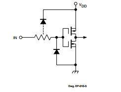
TYPICAL OUTPUT DRIVER TYPICAL INPUT CIRCUIT

FUNCTIONAL BLOCK DIAGRAM


