Active Member
|
[China]

Address: Room 36B1-B2, Building C, Electronics Science & Technology Building Shennan Mid-Road, Shenzhen China
Contact name:Sharon Yang

Anterwell Technology Ltd. |
|
|
FEATURES
• Output capability: standard
• ICC category: flip-flop
GENERAL DESCRIPTION
The 74HC/HCT107 are high-speed Si-gate CMOS devices
and are pin compatible with low power Schottky TTL
(LSTTL). They are specified in compliance with JEDEC
standard no. 7A.
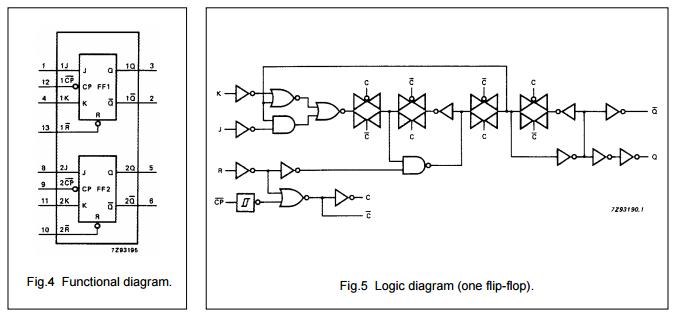
The 74HC/HCT107 are dual negative edge triggered
JK-type flip-flops featuring individual J, K, clock (nCP) and
reset (nR) inputs; also complementary Q and Q outputs.
The J and K inputs must be stable one set-up time prior to
the HIGH-to-LOW clock transition for predictable
operation.
The reset (nR) is an asynchronous active LOW input.
When LOW, it overrides the clock and data inputs, forcing
the Q output LOW and the Q output HIGH.
Schmitt-trigger action in the clock input makes the circuit
highly tolerant to slower clock rise and fall times.
QUICK REFERENCE DATA
GND = 0 V; Tamb = 25 °C; tr = tf = 6 ns
| SYMBOL | PARAMETER | CONDITIONS | TYPICAL | UNIT | |
| HC | HCT | ||||
| tPHL/ tPLH | propagation delay nCP to nQ nCP to nQ nR to nQ, nQ | CL = 15 pF; VCC = 5 V |
16 16 16 |
16 18 17 |
ns ns ns |
| fmax | maximum clock frequency | 78 | 73 | MHz | |
| CI | input capacitance | 3.5 | 3.5 | pF | |
| CPD | power dissipation capacitance per flip-flop | notes 1 and 2 | 30 | 30 | pF |
Notes
1. CPD is used to determine the dynamic power dissipation (PD in µW):
PD = CPD × VCC2 × fi + ∑ (CL × VCC2 × fo) where:
fi = input frequency in MHz
fo = output frequency in MHz
∑ (CL × VCC2 × fo) = sum of outputs
CL = output load capacitance in pF
VCC = supply voltage in V
2. For HC the condition is VI = GND to VCC
For HCT the condition is VI = GND to VCC − 1.5 V.
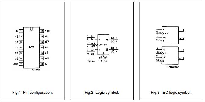
PIN DESCRIPTION
| PIN NO. | SYMBOL | NAME AND FUNCTION |
1, 8, 4, 11 2, 6 3, 5 7 12, 9 13, 10 14 | 1J, 2J, 1K, 2K 1Q, 2Q 1Q, 2Q GND 1CP, 2CP 1R, 2R VCC | synchronous inputs; flip-flops 1 and 2 complement flip-flop outputs true flip-flop outputs ground (0 V) clock input (HIGH-to-LOW, edge-triggered) asynchronous reset inputs (active LOW) positive supply voltage |