

Active Member
|
[China]

Address: 3 / F, building C, jingchengda Industrial Park, Keji 4th Road, Tangtou community, Shiyan town, Bao'an District, Shenzhen City, Guangdong Province
Contact name:Yang

Shenzhen ZYX Science & Technology Co., Ltd. |
|
|
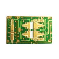
Fast Track Prototyping 8L Led Light Bar Circuit Board Pcb Making Service
Welcome To ZYX
A professional EMS/OEM Manufacturer, ZYX could provide one-stop pcb assembly service,we also could offer:
- Contract Manufacturing
- Engineering Services
- PCB Design & Assembly
- Component Procurement & Material Management
- Product Design
- Fast Track Prototyping
- Cable and Wire Assemblies
- Plastics and Molds
- Function Testing Service
As the Professional PCB Assembly and PCB Manufacturer in China, we pride ourselves on our Excellent Customer Service and Reliability! ZYX also offers Exclusive Services to Help Our Customers with their PCB Projects. Check out our Free PCB Layout Software, our Free PCB File Check and Free PCB Sample.
Model Number: | ZYX-217PFVGFG | Place of Origin: | Shenzhen, China |
Copper Thickness: | 0.5-2oz | Brand Name: | BQZYX+ |
Board Thickness: | 0.1-0.5mm | Min. Line Spacing: | 3mil |
Min. Hole Size: | 0.1-6.5mm | Max Layer: | 8L |
Min. Line Width: | 3mil | Product quotation: | Within 2 Hours |
1. PCB ,FPC , Aluminum PCB ,Membrane Switch ,SMT Stencil Manufacturing
2. PCB, FPC ,Aluminum PCB ,Membrane Switch Copy service
3. Component Sourcing (Supply all electronics)
4. PCB Assembly (Single sided ,double sided and Muli-layer SMT
& PTH& BGA) can Write program for customers
5. PCB PCBA 100% test (X-ray Inspection ,AOI Test , ICT,Probe
flying,burn-in,function test,temperature cycling)
6. Cable&Wire Assemblies&Housing Assemblies
7. Plastics and Molds
8. Better quality and Price for
Heatsink,Cable,Sensor,Modules,Enclosure mold and all Electronic
Parts Cusmized Service

Items | Fabrication Capabilities | Remarks |
Layer Count | 1-10 layers | if your PCB order is over 10 layers, please contact your customer service for quotation. |
Material | FR-4 94V0/ Aluminum | For FPC, HDI, ROGERS, HALOGEN-FREE, HIGH TG ETC., contact your customer service. |
Maximum Size | 500x1100mm | The max. size of PCBGOGO PCB is 50*40cm. and we accept longer PCB board which max. length is 1100MM |
Minimum Size | 3mm*3mm |
|
Maximum Panel Size | 50cm*45cm |
|
Minimum Panel Size | 7.5*7.5cm | If you need v-cut, this is minimum panel size in PCBGOGO |
Tolerance Size of Board | ±0.2mm | CNC tolerance is ±0.2mm, v-cut tolerance is ±0.5mm |
Board Thickness | 0.4-2.4mm |
|
Tolerance Thickness of Board | ±10% | Pay attention: as the capability (PTH, solder mask and others) will add the board thickness, we usually use Plus Tolerance. |
Tolerance Thickness of Board | ±0.1mm | Pay attention: as the capability (PTH, solder mask and others) will add the board thickness, we usually use Plus Tolerance. |
Min. Line Width | 4mil(0.1mm) | Min. Line Width is 0.1mm;In terms of multi-layer PCBs, Min. Line Width for inner-layer is 0.175mm |
0.1mm/4mil for outer layer. If the minimum line width is less than 6 mil, there will be an extra charge / fee. | ||
Min. Line Space | 4mil(0.1mm) | Min. Line Spacing is 0.15mm/6mil. If Min. Line Spacing is less than 6mil, it will charge extra fee. |
Outer Layer Copper Thickness | 35um/70um/105um | It means the thickness of copper in outer layer. 1 OZ=35um, 2OZ=70um, 3OZ=105um. |
Inner Layer Copper Thickness | 35um/50um | Default is 1 OZ, but if you have special requirement, 1.5 OZ is acceptable. |
Drill Diameter Range | 0.2-6.3mm | Min. Size of drill via CNC is 0.2mm. 6.3mm is maximum size. |
Annular Ring | ≥0.1mm(4mil) | If Annular Ring is smaller but there is enough space, there is no limit for the Annular Ring size. But if there is not enough space coupled with dense lines, the Annular Ring size should be over 0.1mm |
Finished Hole Size | 0.2--6.20mm | Because the copper will cover the surface of hole, the Finished hole size is smaller than it is in Gerber file |
The Size Tolerance of Finished | ±0.08mm | Tolerance of Finished Hole Size is ±0.08mm. For example, if the drill in the Gerber file is 0.6mm, the finished drill will be 0.52-0.68mm on standard. |
Solder Mask Type | LPI | LPI is common use in the PCB fabrication. |
Min. Width of Legend | ≥0.15mm | Min. width of legend is 0.15mm, if it is smaller, the legend in the finished board will be not clear. |
Minimum Height of Legend | ≥0.8mm | Min. height of Legend is 0.8mm, if it is smaller, the legend in the finished board will be not clear |
Legend Width/ Height | 1:5 | The suitable proportion of width and height is good for PCB fabrication. |
Space between Trace and | ≥0.3mm(12mil) | Routing: the space between line and frame should be over 0.3mm. V-cut panel: the space between line and v-cut line should be over 0.4mm. |
Panelization | V-scoring, Tab-routing, | Leave min clearance of 1.6mm between boards for break-routing. For V-score panelization, set the space between boards to be zero. |
Min. aperture in half-hole | 0.6mm | Half-hole is a special technology and the min. aperture must be over 0.6 mm |
Q. What service can you supply ?
ZYX are OEM PCB and PCBA manufacturer since 2010 ,we can provide turnkey solutionincluding RD PCB fabrication,SMT and assembly PCBA inside the enclosure,Functiontesting and other value-added service.
Q. What file you need to prepare if you want to get an quotation from us?
For PCB board, you need to prepare files of Gerber file,it should including RS-274X,ODB++, DXF, PCB, PCBDOC etc formats.
For PCBA(PCB with soldered components), except the file for PCB, you also need to prepare the BOM list (components list), Pick and Place file(txt format), real sample pictureor 3D PDF version file etc.
Q. How to keep our product information and design file secret ?
We are willing to sign a NDA effect by customers side local law and promising tokeep customers data in high confidential level.
Q. How about the delivery?
Normally, for sample order, our delivery is about 5 days.For small batch, our delivery is about 7 days.
For mass production batch, our delivery is about 10 days.
But that depends on the real condition when we get your order.
If your order is urgently please contact us directly ,we will priority to deal it and do ourbest to give you satisfied delivery time.
Q. How can we guarantee you receive an good quality product?
For PCB, we will use Flying Probe Test, E-test etc. for it.
For PCBA, we need you to offer us a method or test fixture for the function test.Before that, our inspectors will use microscope and X-ray to check the IC footwelding or bad solder etc.


