Active Member
|
[China]

Address: No.99 Tong Xi Road, Caijia Town, Beibei District, Chongqing,China
Contact name:Wu

Chongqing Silian Optoelectronic Science & Technology Co., Ltd. |
|
|
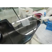
Thickness 650um Dia 100 mm 4 inch Sapphire Substrate Wafer Single Side Polished
Orientation: (22-43)Plane offcut 0.45° away from C plane-per sketch 22-43
Diameter: 100mm ± 0.2mm
Thickness: 650um ± 20um / 850um ± 20um
Bow: <10 microns
Warp: <20 microns
TTV: <10 microns
Major Flat: M-axis +0.3°; 32+1mm
Minor Flat: None
Front Side: < 0.30nm
Back Side: <1.2 microns
Laser ID: marked on backside by major flat
Packaged: Cassette containing 25 wafers(s), Class 100 cleanroom envirnment
Specification
| Orientation | (22-43)Plane offcut 0.45° away from C plane-per sketch 22-43 |
| Diameter | 100mm ± 0.2mm |
| Thickness | 650um ± 20um / 850um ± 20um |
| Bow | <10 microns |
| Warp | <20 microns |
| TTV | <10 microns |
| Major Flat | M-axis +0.3°; 32+1mm |
| Minor Flat | None |
| Front Side | < 0.30nm |
| Back Side | <1.2 micron |
| Laser ID | marked on backside by major flat |
| Packaged | Cassette containing 25 wafers(s), Class 100 cleanroom envirnment |
Customers need to know:
1. The products are made according to the requirements of
customers. Please contact us before placing an order to confirm the
detailed production process, quantity, production period, logistics
and other relevant information.
2. Customization needs to know:
(1) plate Customization: please directly provide dimensions (length * width * thickness, and color quantity) (please consult customer service quotation).
(2) product processing: please send drawings to the owner, such as CDR, AI, CAD and other vector drawings, and inform the thickness, (consult customer service quotation) to give you a quotation. No friends can draw by hand and take photos for us. We need drawings for complex processing.
3. Please confirm the size and drawing carefully before
photographing. Once processed, it will not be returned or changed.
4. There is a certain tolerance for processing and material
thickness. Buyers who require no difference should be merciful! The
tolerance is about 0.3mm. Once photographed, we do not accept any
return or exchange due to tolerance!
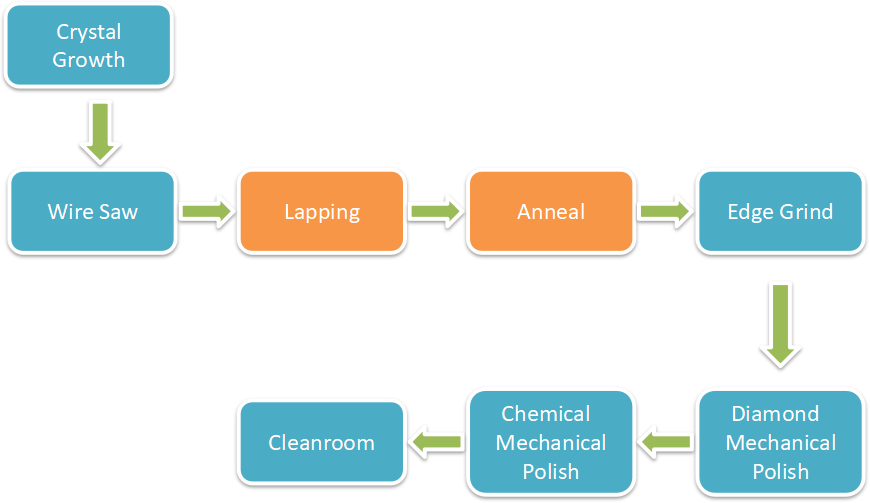
Process Flow