
|
|
[China]

Trade Verify
Address: 4F&2F, Building 1st, Nanchang Huafeng Industrial Park,NanchangCommunity, Xixiang Town, Baoan District, Shenzhen, China
Contact name:Yang

Shenzhen Sky-Win Technology Co., Ltd |
|
Verified Suppliers
|
|
|
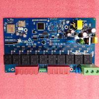
Quick Turn Communication PCB Assembly Electronic 6-Layers PCB High Tg170 and High Tg180 Boards
Communication PCB Assembly Application
PCB requirements in the field of communication can be divided into sub-fields such as communication equipment and mobile terminals. Among them, communication equipment mainly refers to the communication infrastructure used for wired or wireless network transmission, including communication base stations, routers, switches, backbone network transmission equipment, microwave transmission equipment, optical fiber to the home equipment.The following are the most common applications in the telecom industry that make effective use of PCBS:
Wireless communication system
Mobile phone tower system
Telephone switching system
Industrial wireless communication technology
Commercial telephone technology
Electronic data storage devices
Mobile communication system
Satellite systems and communications equipment
Security technology and information and communication systems
Communications PCB Parameters
| Layer: | 8 layers |
| Surface: | HASL/OSP/ENIG/ImmersionGold/Flash Gold/Gold finger ect. |
| Copper thickness: | 0.25 Oz -12 Oz |
| Material: | FR-4,Halogen free,High TG,Cem-3,PTFE,Aluminum BT,Rogers |
| Board thickness | 0.1 to 6.0mm(4 to 240mil) |
| Minimum line width/space | 0.076/0.076mm |
| Minimum line gap | +/-10% |
| Outer layer copper thickness | 140um(bulk) 210um(pcb prototype) |
| Inner layer copper thickness | 70um(bulk) 150um(pcb protytype) |
| Min.finished hole size(Mechanical) | 0.15mm |
| Min.finished hole size (laser hole) | 0.1mm |
| Aspect ratio | 10:01(bulk) 13:01(pcb prototype) |
| Solder Mask Color | Green,Blue,Black,White,Yellow,Red,Grey |
| Tolerance of dimension size | +/-0.1mm |
| Tolerance of board thickness | <1.0mm +/-0.1mm |
| Tolerance of finished NPTH hole size | +/-0.05mm |
| Tolerance of finished PTH hole size | +/-0.076mm |
| Delivery time | Mass:10~12d/ Sample:5~7D |
The PCBA Assembly Process For Communication Equipment Typically Includes The FollowingSteps
PCB design: The first step in PCBA assembly is to design the PCB
according to the specifications and requirements of the
communication equipment
Component selection: After the PCB design is complete, the next
step is to select the components that will be used in the assembly.
This typically includes components such as microprocessors, memory
chips, radio frequency (RF) modules, and other electronic
components.
PCB assembly: The selected components are then assembled onto the PCB using an automatic pickup and placement machine. Place the components onto the PCB and weld them into place using a reflow furnace.
Testing: After the PCB is assembled, the PCBA is tested to ensure that it meets the necessary performance and reliability standards. This includes functional, performance and durability testing.
Quality control: The final step in PCBA assembly is quality control, which includes checking the PCBA for defects and ensuring that it meets the necessary quality standards.


