

Active Member
|
[China]

Address: Room 1520, Block 11, International E-Commerce Logistics Center, PingAn Road, PingHu Street, LongGang District, ShenZhen City, China 518111
Contact name:Steven YU

Witgain Technology Limited |
|
|
Double Layer Printed Circuit Board Pcb 1.6mm Thickness HASL
1 2 Layer FR4 substrate material printed circuit board.
2 Double layer copper, copper thickness is 35um/35um.
3 Finished pcb thickness is 1.6mm.
4 Used in power supply product..
5 HAL Lead Free.
6 2 layer pcb with 10/10mil min line space and width.
7 Green solder mask and white silkscreen.
8 Need customer to send us the gerber file or PCB file
| NO | Equipment Name | Equipment Brand | Equipment QTY |
| 1 | Automatic Cutting | SCHCLLING-CA6858 | 1 |
| 2 | Roll Cutting | QIXIAN | 2 |
| 3 | Vertical Cutting | SHANGYUE | 2 |
| 4 | Innerlayer pretreatment | JIECHI | 4 |
| 5 | Automatic coat&wiring | QUNYU | 4 |
| 6 | Automatic exposure | CHUANBAO | 11 |
| 7 | Large table exposure | HECHUAN | 2 |
| 8 | Laser Plotter | ORBOTEC | 3 |
| 9 | Etching line | KB | 4 |
| 10 | PE Punching | PE-3000 | 1 |
| 11 | AOI | ORBOTEC | 10 |
| 12 | Double row brown | KB | 3 |
| 13 | PP Cutting | ZHENGYE | 5 |
| 14 | PP Chopping | ZHONGDA | 2 |
| 15 | Hot-melt machine | HANSONG | 6 |
| 16 | Riveting machine | JIAOSHI | 6 |
| 17 | X-Ray Check | HAOSHUO | 5 |
| 18 | Automatic reflux | LANDE | 2 |
| 19 | Steel plate washer | FENGKAI | 2 |
| 20 | Large size press | DATIAN | 8热4冷 |
| 21 | X-Ray Drilling target | HAOSHUO | 8 |
| 22 | Ccd Drilling target | XUELONG | 10 |
| 23 | Automatic grinding | XINHAO | 5 |
| 24 | Plate thickness Measuring | AISIDA | 2 |
| 25 | Four axis gongs machine | DALIANG | 2 |
| 26 | Two axis gongs machine | BIAOTEFU | 4 |
| 27 | Automatic grinding mill | JIEHUI | 2 |
| 28 | Drilling machine | TONGTAI | 13 |
| 29 | Hole testing machine | YAYA | 1 |
| 30 | Sinking rough mill | KB | 1 |
| 31 | Vertical copper wire | YAMEI | 1 |
| 32 | Automatic electroplating line | JINMING | 1 |
| 33 | Dryer after electroplating | KB | 1 |
| 34 | Etch machine | KB | 1 |
| 35 | Film checking machine | YUBOLIN | 2 |
| 36 | Line pre-processing | KB | 2 |
| 37 | Automatic laminator | ZHISHENG | 3 |
| 38 | Outer exposure machine | CHUANBAO | 8 |
| 39 | Outer exposure machine | HECHUAN | 3 |
| 40 | Etch machine | JULONG | 1 |
| 41 | Line developing machine | KB | 1 |
| 42 | Sand blasting machine | KB | 1 |
| 43 | Precoarsening pretreatment | KB | 2 |
| 44 | Electrostatic spraying line | FURNACE | 1 |
| 45 | Automatic screen printing machine | HENGDAYOUCHUANG | 12 |
| 46 | Pre baked tunnel furnace | KB | 1 |
| 47 | Solder resist exposure machine | CHUANBAO | 6 |
| 48 | Solder resist exposure machine | HECHUAN | 2 |
| 49 | Post baked tunnel furnace | GC0-77BD | 2 |
| 50 | Solder resist developing machine | KB | 1 |
| 51 | Screen printing machine | 1.8mm/2.0mm | 4 |
| 52 | Character baking tunnel furnace | GC0-77BD | 1 |
| 53 | Sunk Tin spray line | 2 | |
| 54 | Nickel palladium and gold wire | XINHUAMEI | 1 |
| 55 | Alternator | 2 | |
| 56 | OSP line | KB | 1 |
| 57 | Gongs machine | YIHUI | 20 |
| 58 | V-CUT | ZHENGZHI | 1 |
| 59 | CNC V-CUT machine | CHENGZHONG | 2 |
| 60 | Hydraulic punch press | SRT | 2 |
| 61 | Test machine | MASON | 17 |
| 62 | High speed flying needle tester | WEIZHENGTAI | 3 |
| 63 | Four wire flying needle tester | XIELI | 2 |
| 64 | Product washing machine | KB | 2 |
| 65 | Plate warping machine | XINLONGHUI | 2 |
| 66 | Vacuum packaging machine | SHENGYOU | 4 |
Q1:
Q1: What is the Comparative Tracking Index (CTI) or Proof Tracking Index (PTI) of the PCB base material?
A1:
Comparative Tracking Index (CTI) is the extent to which the insulating material of the PCB can resist the unwanted current to flow between traces on the board. It is a measure of the ability of the PCB substrate to withstand any breakdown between two tracks on the PCB surface. It is used to assess the proportionate resistance of the PCB base material and helps calculate the high-voltage isolation values between the tracks. The CTI / PTI value indicates how resistant the PCB material is against environmental influences such as dirt and moisture. The higher the value, the more resistant the material is. The default CTI value for FR4 is 175 and goes up to 600 on special materials. The CTI / PTI value is determined using standard test methods.
Tracking resistance is the resistance offered by the PCB trace against the current flow. The higher the number of components placed on the PCB board the higher is its overall packing density, this leads to smaller trace spacings. Therefore, the CTI / PTI value in the PCB base material is of prime importance. These values help to deduce the overall PCB tracking resistance.
These values give an estimation for leakage or short-circuit as trace spacing becomes small due to the increased number of components. As per the IEC standard, the smaller CTI grade substrate offers good resistance to the electrical breakdown. CTI is a critical number while selecting a PCB material. Normal FR-4 ranges from 175 to 225V. IEC has prescribed three of the following classes for PCB CTI calculation:
| Comparative Tracking Index (CTI) in Volts | Class |
| 600 <= CTI | I |
| 400 <= CTI < 600 | II |
| 175 <= CTI < 400 | IIIA |
| 100 <= CTI < 175 | IIIB |
Understanding CTI with respect to PCB routing:
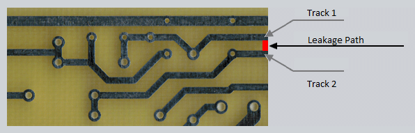
When two PCB traces run in parallel, the dielectric material should not breakdown at any time and both traces should be able to carry current without any problem. The chance of dielectric breaking down and the traces having a direct short is very less. The dielectric ensures that resistance is present between the two traces. One of the primary reasons why the two traces might have leakage current is due to the impurities forming between traces, environmental conditions, voltage applied, and temperature..
CTI is the measurement of the susceptibility of the PCB’s insulating material to the electrical breakdown. Mathematically, CTI is that voltage, which results in failure by breakdown after 50 drops of 0.1 percent ammonium chloride solution have fallen on the material.
Creepage Distance and CTI Value:
Creepage distance is the shortest path available between two PCB conductors measured along the surface of the insulation. Depending upon the CTI value of the PCB base material, the creepage value will differ. If the CTI value is higher, then the minimum creepage value is required. In short, high a CTI value indicates closeness between the PCB conductors.


