

Active Member
|
[China]

Address: Room 1520, Block 11, International E-Commerce Logistics Center, PingAn Road, PingHu Street, LongGang District, ShenZhen City, China 518111
Contact name:Steven YU

Witgain Technology Limited |

|
|
4 Layer 2 OZ CU PCB With TG170 FR4 Material Printed Circuit Board
1 4 Layer Printed Circuit Board PCB .
2 Immersion Gold treatment, gold thickness 2u'.
3 FR4 substrate material, tg170 degree.
4 Min line space and width 5/5mil.
5 Copper thickness is 2 OZ on out layer, 1 OZ on inner layer
6 Greensolder mask and white silkscreen.
7 ROHS, MSDS, SGS, UL, ISO9001&ISO14001 Certificated
8 Application product: Industrial Control
| S1150G | |||||
| Items | Method | Condition | Unit | Typical Value | |
| Tg | IPC-TM-650 2.4.25 | DSC | ℃ | 155 | |
| Td | IPC-TM-650 2.4.24.6 | 5% wt. loss | ℃ | 380 | |
| CTE (Z-axis) | IPC-TM-650 2.4.24 | Before Tg | ppm/℃ | 36 | |
| After Tg | ppm/℃ | 220 | |||
| 50-260℃ | % | 2.8 | |||
| T260 | IPC-TM-650 2.4.24.1 | TMA | min | >60 | |
| T288 | IPC-TM-650 2.4.24.1 | TMA | min | 30 | |
| Thermal Stress | IPC-TM-650 2.4.13.1 | 288℃, solder dip | -- | pass | |
| Volume Resistivity | IPC-TM-650 2.5.17.1 | After moisture resistance | MΩ.cm | 6.4 x 10⁷ | |
| E-24/125 | MΩ.cm | 5.3 x 10⁶ | |||
| Surface Resistivity | IPC-TM-650 2.5.17.1 | After moisture resistance | MΩ | 4.8 x 10⁷ | |
| E-24/125 | MΩ | 2.8 x 10⁶ | |||
| Arc Resistance | IPC-TM-650 2.5.1 | D-48/50+D-4/23 | s | 140 | |
| Dielectric Breakdown | IPC-TM-650 2.5.6 | D-48/50+D-4/23 | kV | 45+kV NB | |
| Dissipation Constant (Dk) | IPC-TM-650 2.5.5.9 | 1MHz | -- | 4.8 | |
| IEC 61189-2-721 | 10GHz | -- | — | ||
| Dissipation Factor (Df) | IPC-TM-650 2.5.5.9 | 1MHz | -- | 0.01 | |
| IEC 61189-2-721 | 10GHz | -- | — | ||
| Peel Strength (1Oz HTE copper foil) | IPC-TM-650 2.4.8 | A | N/mm | — | |
| After thermal Stress 288℃,10s | N/mm | 1.4 | |||
| 125℃ | N/mm | 1.3 | |||
| Flexural Strength | LW | IPC-TM-650 2.4.4 | A | MPa | 600 |
| CW | IPC-TM-650 2.4.4 | A | MPa | 450 | |
| Water Absorption | IPC-TM-650 2.6.2.1 | E-1/105+D-24/23 | % | 0.1 | |
| CTI | IEC60112 | A | Rating | PLC 0 | |
| Flammability | UL94 | C-48/23/50 | Rating | V-0 | |
| E-24/125 | Rating | V-0 | |||
Q1: What are black pads on a pcb? What are black pads in ENIG
finish?
A1:
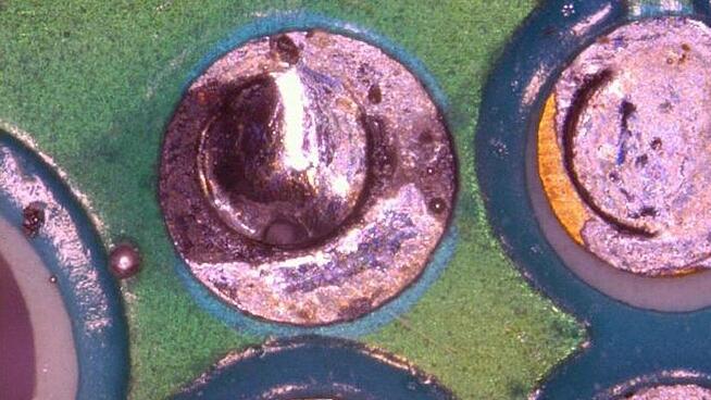
Black pads are primarily a layer of dark nickel that is formed due to corrosion on the surface of a PCB that has an ENIG (Electroless Nickel and Immersion Gold) finish. Black Pads are the result of excessive phosphorous content reacting with gold during the gold deposition process which is an essential step in applying an ENIG finish.
ENIG is a surface finish that is applied on the printed circuit boards (PCBs) after solder mask application to provide an additional layer of finish/coating on all exposed copper surfaces and sidewalls. Additionally, it helps avoid oxidation and improves the solderability of copper contacts and plated through-holes.
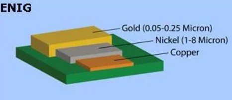
ENIG coating requires 93% of the pure nickel which is applied over the PCB’s surface and also a considerate amount of phosphorous (6 to 8%). It is important to moderate the amount of phosphorous and factor in the possibility of how many times a given PCB will be soldered again as this might increase the phosphorous content and will form a black pad.
Immersion Gold is applied after the nickel deposition process. The Gold provides a considerate coating on all exposed layers. The nickel deposition acts as a barrier between copper and gold, which prevents unwanted unsolderable blots on the PCB’s surface. The Nickel deposition also adds strength to plated through holes and vias.
While the ENIG produces a highly solderable finish, the process of applying the ENIG coating inconsistently creates a black pad which results in reduced solderability and weakly formed solder joints of the PCB.
What Causes Black Pads?
High phosphorus content: An ENIG finished PCB has a longer shelf life but over time some nickel can dissolve leaving behind its by-product which is phosphorous. The amount of phosphorous content increases with reflow soldering. The higher the level of phosphorous, the greater the risk of formation of black pads during the Gold deposition process.
Corrosion during gold deposition: The ENIG process relies on a corrosion reaction when the gold is to be deposited on the nickel surface. It is essential that the gold deposition is not aggressive, as it can increase the corrosion to the level where a black pad is formed.
How to prevent Black pads?
Preventing black pads is an essential step for PCB manufacturers. As observed black pads are caused due to higher levels of phosphorous, so it is essential to control the nickel bath concentration during the metal plating process during the manufacturing stage. Additionally, black pads are also formed due to an aggressive amount of gold deposition. Hence it is essential to maintain strict control over the amount of nickel and gold that is being used.


