

Active Member
|
[China]

Address: Block 11, International E-Commerce Logistic Center, PingHu Street, LongGang Distric, ShenZhen City
Contact name:Steven

Witgain Technology Ltd |
|
|
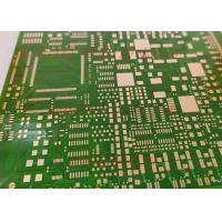
10 Layer Printed Circuit Board With Blind And Buried Holes
PCB Specifications:
PCB Type: HDI PCB ( High Density Interconnector)
Layer Count: 10 Layer
Board Thickness: 1.8MM
Material: FR4 IT180A IT-180ATC-Data-sheet-rev-2.0-20-1.pdf
Min Hole: 0.1MM
Min Line: 3/3 Mil
BGA Size: 10Mil
Unit Size: 154MM*143MM/1UP
Blind Holes: L1-L2 , L9-L10 0.1MM
Buried Holes: L2-L9 0.2MM
Via Holes: L1-L10 0.2MM
Solder Mask: Green
Surface Treatment: ENIG
Application: Motor Industrial Control
Our Capability:
| NO | Item | Capability |
| 1 | Layer Count | 1-24 Layers |
| 2 | Board Thickness | 0.1mm-6.0mm |
| 3 | Finished Board Max Size | 700mm*800mm |
| 4 | Finished Board Thickness Tolerance | +/-10% +/-0.1(<1.0mm) |
| 5 | Warp | <0.7% |
| 6 | Major CCL Brand | KB/NanYa/ITEQ/ShengYi/Rogers Etc |
| 7 | Material Type | FR4,CEM-1,CEM-3,Aluminum,Copper, Ceramic, PI, PET |
| 8 | Drill Hole Diameter | 0.1mm-6.5mm |
| 9 | Out Layer Copper Thickness | 1/2OZ-8OZ |
| 10 | Inner Layer Copper Thickness | 1/3OZ-6OZ |
| 11 | Aspect Ratio | 10:1 |
| 12 | PTH Hole Tolerance | +/-3mil |
| 13 | NPTH Hole Tolerance | +/-1mil |
| 14 | Copper Thickness of PTH Wall | >10mil(25um) |
| 15 | Line Width And Space | 2/2mil |
| 16 | Min Solder Mask Bridge | 2.5mil |
| 17 | Solder Mask Alignment Tolerance | +/-2mil |
| 18 | Dimension Tolerance | +/-4mil |
| 19 | Max Gold Thickness | 200u'(0.2mil) |
| 20 | Thermal Shock | 288℃, 10s, 3 times |
| 21 | Impedance Control | +/-10% |
| 22 | Test Capability | PAD Size min 0.1mm |
| 23 | Min BGA | 7mil |
| 24 | Surface Treatment | OSP, ENIG,HASL, Plating Gold, Carbon Oil,Peelable Mask etc |
FAQ:
Question: What is Glass Transition Temperature (Tg)?
Answer:Tg or the glass transition temperature is the temperature at which the base material of a PCB starts to transform from a brittle/rigid form factor to a soft, elastic one. The Tg value of a printed circuit board usually depends on the substrate used. This is one of the factors that you must consider when selecting the substrate materials for your PCB. You should make sure that the temperature where your board will be used is about 20 degrees less than the Tg value of the selected substrate.
Quesion: What is the Wetting Balance Test?
Answer: The Wetting Balance Test is conducted to measure the wetting forces between molten solder and the PCB as a function of time. The wetting balance test measures the time it takes for the solder to wet the termination pads of the component on a PCB.
During the test, the PCB is inserted into and removed from a molten solder pot at high speeds (1 to 5 mm/ sec). The solder pot is held steady for 5 to 10 seconds while the PCB is inserted and removed in the vertical dimension. Forces like surface tension and buoyancy act on the board in the vertical dimension.
The net active forces are measured using a linear variable differential transformer (LVDT) and used to draw a wetting balance curve to show the total force (mN) or normalized force (mN/mm) as a function of time. It provides information about the extent of wetting.

Apart from wetting forces, there are rejecting (non-wetting) forces too, as plotted in the figure on the negative axis. The rejecting forces act in the upward direction and the wetting forces act in the downward direction.
The rate of insertion of specimen is high enough that it reaches the depth of the solder pot before the wetting forces came into action. Initially, the rejecting forces are high, that’s why the curve rises from the negative axis. After some time, the wetting forces overcome the rejecting forces, which is depicted by the curve on the positive axis. The point where the magnitude of both the forces match each other, they cross the zero-axis called Time-to-Zero. When solder sticks to the PCB specimen, it compels it to move downward, resulting curve movement in the positive direction. The slope of the rising curve gives the indication of the wetting rate.
The Wetting Balance test is fast, automated, and an entirely qualitative method, which only specifies whether the specimen under test has passed/ failed. We need a statistically-proven test method to get clear-cut information on solderability validation. For solderability evaluation, the wetting curve is divided into three pass/fail valuations based on IPC-J-STD-003 criteria.


