

Active Member
|
[China]

Address: Block 11, International E-Commerce Logistic Center, PingHu Street, LongGang Distric, ShenZhen City
Contact name:Steven

Witgain Technology Ltd |
|
|
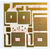
1 Layer Ceramic Printed Circuit Board , AL2O3 Material , Board Thickness 2.0MM
PCB Specifications:
Layer Count: 1 Layer Ceramic PCB
Board Thickness: 1.6MM
Material: AL2O3, Ceramic
Copper Thickness: 1OZ
Application: Work in high temperture condition
Capabilities:
| Item | Capability |
| Layer Count | 1-24 Layers |
| Board Thickness | 0.1mm-6.0mm |
| Finished Board Max Size | 700mm* 800mm |
| Finished Board Thickness Tolerance | +/-10% +/-0.1(<1.0mm) |
| Warp | <0.7% |
| Major CCL Brand | KB/NanYa/LTEQ/ShengYi/Rogers Etc |
| Material Type | FR4,CEM-1,CEM-3,Aluminum,Copper,Ceramic, PI, PET |
| Drill Hole Diameter | 0.1mm-6.5mm |
| Out Layer Copper Thickness | 1/20Z-8OZ ; |
| Inner Layer Copper Thickness | 1/3OZ-6OZ |
| Aspect Ratio | 10:1 |
| PTH Hole Tolerance | +/-3mil |
| NPTH Hole Tolerance | +/-1mil |
| Copper Thickness Of PTH Wall | >10mil(25um) |
| Line Width And Space | 2/2mil |
| Min Solder Mask Bridge | 2.5mil |
| Solder Mask Alignment Tolerance | +/-2mil |
| Dimension Tolerance | +/-4mil |
| Max Gold Thickness | 200u'(0.2mil) |
| Thermal Shock | 288C, 10s, 3 Times |
| Impedance Contro | +/-10% |
| LTest Capability | PAD Size Min 0.1mm |
| Min BGA | 7mil |
| Surface Treatment | OSP, ENIG, HASL, Plating Gold, Carbon Oil,Peelable |
FAQ:
Question: What is the main feature for Ceramic pcb?
Answer: 1) High Rockwell Hardness, about HRA80-90
2) Good wear-resisting property
3) Small density, about 3.5g/cm2
4) High melting point: over 1000C
5) Good corrosion resistance: it is very steady in strong acid and strong alkali condition
Question: What is the application area of Ceramic pcb?
Answer: Because ceramic pcb has very excellent physical stability and anticorrosion features, it can be used in a lot of areas, like automobiles, arerospace, LED light , semiconductor module, communications, solar energy batteries etc.
Exhibitions:


