

Active Member
|
[China]

Address: Room 126-305, Building 2, Lixinhu Creative Park, No.1 Furui Road, Fuhai Subdistrict Bao'an District, Shenzhen, Guangdong, China
Contact name:Damon Liu

Shenzhen Betterliv Technology Co., Ltd. |
|
|
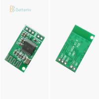
Bluetooth Module PCB Layout Add Bluetooth To Keyboard PCB Design Bluetooth Receiver Module PCB
PCB Capability
Layers | Single Sided,2 to 18 Layer |
Board material type | FR4,CEM-1,CEM-3,ceramic substrate board, aluminum based board, high-Tg, Rogers and more |
Maximum dimension | 610 x 1,100mm |
PCB assembly process: | Drilling-----Exposure-----Plating-----Etaching &
Stripping-----Punching-----Electrical Testing-----SMT-----Wave Soldering-----Assembling-----ICT-----Function Testing-----Temperature & Humidity Testing |
Files needed | PCB: Gerber files(CAM, PCB, PCBDOC) |
Components: Bill of Materials(BOM list) | |
Assembly: Pick-N-Place file | |
Passive Down to 0201 size | |
BGA and VFBGA | |
Leadless Chip Carriers/CSP | |
Double-sided SMT Assembly | |
Fine Pitch to 0.8mils | |
BGA Repair and Reball | |
Part Removal and Replacement |
Our advantages
1. High-end, Small volume and Various kinds of PCBA service
offered;
2. Speedy, Flexible and one-stop service in PCBA;
3. Assembly and Purchasing service offered, all components are
promised to be purchased 100% from Original factories or their
pointed agents;
4. Transparent quotation,cost and benefit are detailedly opened to
customer;
5. With professional Engineers and Long-term successful experience
in cooperating with customers inland and overseas, all new projects
can be developed faster and better than expected;
6. With USA or Japan imported tin cream and tin bar, and 100% AOI
testing during production,
All PCBAs we made are more reliable.


