
|
|
[China]

Trade Verify
Address: Room 1106, CIBC, No.198 Wuxing Rd, Hangzhou, P.R.China
Contact name:Xu

Hangzhou Freqcontrol Electronic Technology Ltd. |
|
Verified Suppliers
|

|
|
Highly Stable Sapphire Wafer for Consistent Optical Properties C-plane 0001
the Sapphire Wafer - a Unique Innovation in High-Tech Materials
Step into the future with our revolutionary Sapphire Wafer, a cutting-edge product that revolutionizes the world of semiconductors and optoelectronics. This wafer, crafted from pure sapphire, offers unparalleled durability and transparency, making it ideal for a wide range of applications.
The Sapphire Wafer's exceptional hardness and resistance to scratching ensure long-lasting performance, even in the most demanding environments. Its high thermal conductivity effectively dissipates heat, preventing overheating and enhancing overall stability.
Moreover, the wafer's optical properties are second to none, offering superior clarity and transmittance. This makes it a perfect choice for optoelectronic devices such as LEDs, lasers, and sensors.
With its superior performance and versatility, the Sapphire Wafer is poised to become a game-changer in the high-tech industry. Don't miss out on this opportunity to embrace the future of technology. Invest in the Sapphire Wafer today and experience its remarkable benefits.


OPTICAL PROPERTIES
Transmission | 0.17 to 5.5 um |
Refractive Index | 1.75449 (o) 1.74663 (e) at 1.06 um |
Reflection Loss | at 1.06 microns (2 surfaces) for o-ray - 11.7%; for e-ray - 14.2% |
Absorption Index | 0.3 x 10⁻³ cm-1 at 2.4 um |
dN/dT | 13.7 x 10⁻⁶ at 5.4 um |
dn/dm = 0 | 1.5 um |
Orientation | R-plane, C-plane, A-plane, M-plane or a specified orientation |
Orientation Tolerance | ± 0.3° |
Diameter | 2 inches, 3 inches, 4 inches, 6 inches, 8 inches or others |
Diameter Tolerance | 0.1mm for 2 inches, 0.2mm for 3 inches, 0.3mm for 4 inches, 0.5mm for 6 inches |
Thickness | 0.25mm, 0.33mm, 0.43mm, 0.65mm, 1mm or others; |
Thickness Tolerance | 25μm |
Primary Flat Length | 16.0±1.0mm for 2 inches, 22.0±1.0mm for 3 inches, 30.0±1.5mm for 4 inches, 47.5/50.0±2.0mm for 6 inches |
Primary Flat Orientation | A-plane (1 1-2 0 ) ± 0.2°; C-plane (0 0-0 1 ) ± 0.2°, Projected C-Axis 45 +/- 2° |
TTV | ≤10µm for 2 inches, ≤15µm for 3 inches, ≤20µm for 4 inches, ≤25µm for 6 inches |
BOW | ≤10µm for 2 inches, ≤15µm for 3 inches, ≤20µm for 4 inches, ≤25µm for 6 inches |
Front Surface | Epi-Polished (Ra< 0.3nm for C-plane, 0.5nm for other orientations) |
Back Surface | Fine ground (Ra=0.6μm~1.4μm) or Epi-polished |
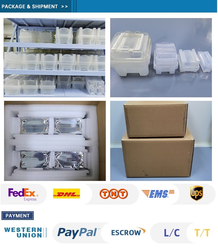
Packaging | Packaged in a class 100 clean room environment |
Acceptance Check

1. The product is fragile. We have adequately packed it and labeled it fragile. We deliver through excellent domestic and international express companies to ensure transportation quality.
2. After receiving the goods, please handle with care and check whether the outer carton is in good condition. Carefully open the outer carton and check whether the packing boxes are in alignment. Take a picture before you take them out.
3. Please open the vacuum package in a clean room when the products are to be applied.
4. If the products are found damaged during courier, please take a picture or record a video immediately. DO NOT take the damaged products out of the packaging box! Contact us immediately and we will solve the problem well.


