

Active Member
|
[China]

Address: Room 704-3, 7 / F, Building 9, Yard 8, Development Road, Changping District, Beijing
Contact name:Marina

Beijing Haina Lean Technology Co., Ltd |
|
|
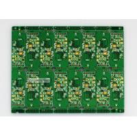
The High-Density Interconnect (HDI) Printed Circuit Boards is shorted as HDI PCB Board.
With little space between the PCB components, and making the board space smaller, at the same time the board functionally isn’t affected.
That is, a PCB with about 120 – 160 pins per square inch is an HDI PCB. All of the other electronic components are mounted on the printed circuit boards(PCBs),which are the foundation.
| Base material | FR4,High-TG FR4,CEM3,aluminum, High frequency(Rogers,Taconic,Aron,PTFE,) |
| Layers | 1-46 |
| Copper Thickness | 0.3oz,0.5oz, 1oz, 2oz, 3oz,4oz,5oz, 6oz |
| Dielectric Thickness | 0.05mm, 0.075mm, 0.1mm,0.15mm,0.2mm |
| board Core Thickness | 0.4mm,0.6mm, 0.8mm, 1.0mm, 1.2mm, |
| 1.5mm, 2.0mm, 3.0mm and 3.2mm | |
| Board Thickness | 0.3mm - 4.0mm |
| Thickness Tolerance | +/-10% |
| Surface Finishing | HASL lead free,ENIG,Plated Gold,Immersion Gold,OSP |
| Solder Mask Color | Green, Blue, Black, White, Yellow, Red, Matt Green, Matt Black, Matt Blue |
| Legend Color | Black, White etc |
| Assembly Types | Surface mount |
| Thro-hole | |
| Mixed technology (SMT & Thru-hole) | |
| Single or double sided placement | |
| Conformal coating | |
| Shield cover assembly for EMI emission control | |
| Parts Procurement | Full Turnkey, Partial Turnkey, Kitted / Consigned |
| Component types | SMT 01005 or larger |
| BGA 0.4mm pitch, POP (Package on Package) | |
| WLCSP 0.35mm pitch | |
| Hard metric connectors | |
| Cable & wire | |
| Other Techniques | Free DFM Review |
| Box Build Assembly | |
| 100% AOI test and X-ray test for BGA | |
| Components cost-down | |
| Function test as custom | |
| Protection technology |
1.through vias from surface to surface,
2.with buried vias and through vias,
3.two or more HDI layer with through vias,
4.passive substrate with no electrical connection,
5.coreless construction using layer pairs
6.alternate constructions of coreless constructions using layer
pairs.

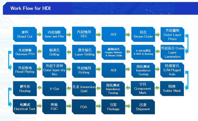
Board Cut - Inner Wet film -DES - AOI - Brown Oxido - Outer Layer Press - Out Layer Lamination - X-RAY & Rounting - Copper reduce & brown oxide - Laser Drilling - Drilling - Desmear PTH - Panel plating - Outer Layer dry film - Etching - AOI- Impedance Testing - S/M Pluged hole - Solder Mask - Component Mark - Impedance testing - Immersion Gold -V-cut - Routing - Electrical Test - FQC - FQA -Package -Shipment
Similar products


| Product Type | Qty | Normal lead time | Quick-turn lead time |
| SMT+DIP | 1-50 | 1WD-2WD | 8H |
| SMT+DIP | 51-200 | 2WD-3WD | 1.5WD |
| SMT+DIP | 201-2000 | 3WD-4WD | 2WD |
| SMT+DIP | ≥2001 | 4WD-5WD | 3WD |
| PCBA(2-4Layer) | 1-50 | 2.5WD-3.5WD | 1WD |
| PCBA(2-4Layer) | 51-2000 | 5WD-6WD | 2.5WD |
| PCBA(2-4Layer) | ≥2001 | ≥7WD | 5WD |
| PCBA(6-10Layer) | 1-50 | 3WD-4WD | 2.5WD |
| PCBA(6-10Layer) | 51-2000 | 7WD-8WD | 6WD |
| PCBA(10-HDILayer) | 1-50 | 7WD-9WD | 5WD |
| PCBA(10-HDILayer) | 51-2000 | 9WD-11WD | 7WD |
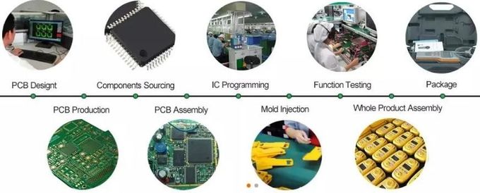
Our products are widely used in communication equipment, industrial control, consumer electronics, medical equipment, aerospace, light-emitting diode lighting, automotive electronics etc.

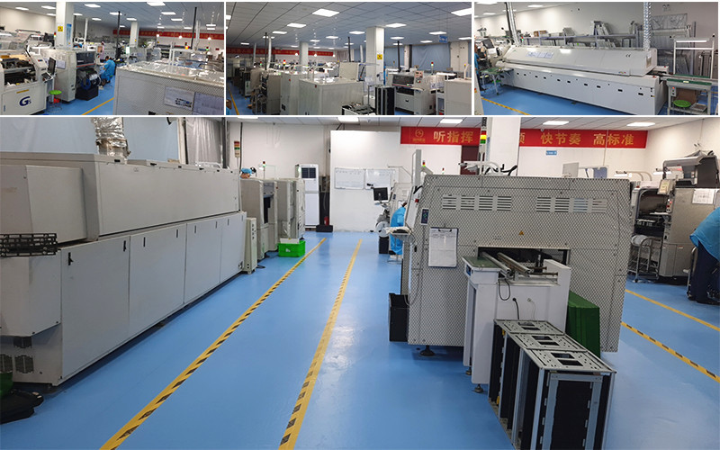
Workshop


1.PCB: Vacuum packaging with carton box
2.PCBA: ESD packaging with carton box

Q1:What kind of PCB file format can you accept for production?
Gerber, PROTEL 99SE, PROTEL DXP, CAM350, ODB+(.TGZ)
Q2:Is my PCB files safe when I submit them to you for manufacturing?
We respect customer's copyright and will never manufacture PCB for someone else with your files unless we receive written permission from you, nor we'll share these files with any other 3rd parties.
Q3:What payments do you accept ?
-Telex Transfer(T/T),Western Union,Letter of Credit(L/C)
-Paypal,AliPay,Credit Card
Q4:How to get the PCB?
A:For small packages, we will ship the boards to you by
DHL,UPS,FedEx,EMS. Door to door service! You will get your PCBs at
your home.
B:For heavy goods more than 300kg, we may ship your boards by ship
or by air to save freight cost. Of course, if you have your own
forwarder, we may contact them for dealing with your shipment.
Q5:What is your minimum order quantity?
Our MOQ is 1 PCS.
Q6: Can we visit your company?
No problem. You are welcome to visit us in Beijing. Or the branch factory is in Tianjin.
Q7: How can you ensure the quality of the PCB?
Our PCBs are 100% test including Flying Probe Test, E-test and AOI.


