
|
|
[China]

Trade Verify
Address: www.pcbseparator.com
Contact name:Alan

Dongguan Chuangwei Electronic Equipment Manufactory |
|
Verified Suppliers
|

|
|
PCB Wave Solder Pallet with Durostone Material Assembly Reflow
BENEFITS
Easy to Use
1) Designed by engineers with extensive wave solder experience
2) Optimized for easy profiling
3) Supports rapid set-up using our ergonomically designed fasteners
4) Optimized for best soldering
5) Wave solder automation to solder through-hole components on
complex electronic assemblies.
Brief introduction
CW Engineering specializes in Wave Solder Pallet For PCB Assembly. Designed by engineers with extensive wave solder experience, our pallets enable customers to automate the soldering of through-hole components on complex electronic assemblies.
The pallets only expose areas of the assembly that require
soldering. All other areas are protected, eliminating component
damage and expensive, low quality process steps. Made of ESD-safe
composite materials, these pallets are designed and manufactured to
optimize both the solder ability of your circuit boards and your
entire process flow.
Specification
Name: Wave solder pallets
Type: CW-Pallet-03
Pallet Material: Durostone anti-static sheet
Sample Availability : Yes
Delivery Terms : Exw ,CIF,CFR
Delivery Lead Times : 3~10
working days
Payment Terms : T/T
Min Quantity : 10
Surface-mount technology (SMT) is the leading factor driving higher circuit densities per square inch on PCBs. Directly attaching components and devices to the surface of circuit boards has enabled products to perform with much higher circuit speeds, allowed greater circuit density, and requires fewer external connections. These advances have greatly lowered costs, improved performance and product reliability. However, these benefits do not come without their challenges. Printing solder paste on diminishing pad sizes, placing smaller components, and reflowing entire assemblies with their varieties of termination finishes and materials are just a few of the technical challenges that process engineers face every day.
Specification:
| Model | DurostoneCHP760 | DurostoneCAS761 | DurostoneCAG762 |
| Grade | Standard | Anti-Static | Anti-static(Optical) |
| Colour | Blue | Black | Grey |
| Density(g/mm3) | 1.85 | 1.85 | 1.85 |
| Standard OperationTemperature | 260 | 260 | 260 |
| Maximum Operation Temperature(C) | 350 | 350 | 350 |
| Sheet Size(mm) | 2440×1220 | 2440×1220 | 2440×1220 |
| Tickness/weight(mm/kg) | 3/17, 4/22 | 5/28, 6/33, 8/44 | 10/55, 12/66 |

Used by most of our customers because of some advantages:
1. Faster positioning on production line
2. Low costs due to the missing of reinforced bars
3. Better volume stocking
4. Better yield with different board type on the production line
Our sales network
This estimation may be done in three ways
If a PCB is available (preferably populated) - our sales engineers
can rapidly evaluate your board.
If PCB design data is available we will process, analyse and
remotely assess it.
You can do it using the rules presented below - our customers
quickly find that the above two methods are easiest.
Gerber, Excellon and other data required
Pin Land to SMT pad clearance evaluation
The two figures below each show part of a CSWSC in plan and section
views. The right hand figure shows that more clearance
is required when the connector orientation is perpendicular to the
wave.
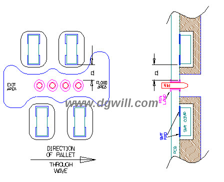
PTH Components Located Parallel to direction through wave
The clearance required between the pin land and SMT pad can be made
quite
small, as the solder does not have to flow "under" the component
pockets.

PCB Design Implications - for Board Designers - or respin
We are often called upon by our customers to help with identifying design respin opportunities.
We will identify problem areas within a board and suggest appropriate movements of components. (Ideally before the PCB is fabricated)
However for board designers reading this, can you remember another
four "rules" (to compete with the hundred other rules you have to
have floating
around in your head).
Keep large (height) SMT components away from PTH areas.
Leave the leading and trailing areas around PTH components as clear
as possible.
DON'T put any SMT components within 3mm (0.12") of any PTH
components.
DON'T put all PTH components in line along one edge of a board -
leave some space to allow us to support the masking in the centre
of the board.
More information welcome to contact us:
Email/Skype: s5@smtfly.com
Mobile/Wechat/WhatsApp(Bunny): +86-136-8490-4990


