Active Member
|
[China]

Address: Huishang Building, 19-128 Nathan Road, Yau Tsim Sha Tsui, Yau Tsim, Hong Kong
Contact name:Mank.Li

Shenzhen Chaosheng Electronic Technology Co.,Ltd |
|
|
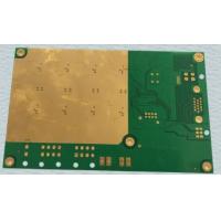
10 layer gold immersion rigid PCB board layout HASL 1 OZ Squre Board For industrial control
RF PCB – Radio Frequency Printed Circuit Boards
Call us or get an instant PCB quote. Tell our experts what you need and we will provide you with the right PCB fabrication and PCB assembly solution. We are ready and eager to turn your concepts into reality.
The main difference between RF circuit boards and Microwave PCBs is in the radio frequency in which they operate. Microwave PCBs are classified as any RF circuit board operating above 2GHz.
RF circuit boards and Microwave PCBs are used for communication signals in any application that requires receiving and transmitting radio signals. For example, some common applications are cell phones and radar installations.Microwave PCB and RF Circuits–Common Problems and Solutions
RF circuit boards, and Microwave PCBs, are especially difficult to design compared to traditional PCB layouts. This is due to the problems that could arise in receiving or transmitting the radio signals. Some of the main problems are noise sensitivity, and tighter impedance tolerances
Compared to traditional circuit boards, radio and microwave signals are very sensitive to noise and also require much tighter impedance tolerances. The best solution for these problems is to utilize ground plans and use a generous bend radius on impedance controlled traces. These solutions will ultimately allow the RF/Microwave PCB to achieve the best performance.
RF boards have a multitude of different applications, including wireless technologies, smart phones, sensors, robotics and security. With the advent of new technologies that are pushing the limits of electronics, the demand for RF boards is on the rise.
Finding a capable RF PCB manufacturer is critical to make sure the boards are fabricated to high quality standards and on-time. Our reputation speaks for itself. We pride ourselves on bringing the most demanding layout concepts to reality.
We can help with everything from saving cost on a simple board to manufacturing advice for cutting edge, fifty layer designs. To simplify your search, here are several recommendations for materials based on application and manufacturability:
Important Note: Within every industry, there is a wide range of applications, demands, and budgets.
The table below provides general recommendations, but to find the best PCB materials for your specific project, please contact our engineering staff.
| RF Application | RF Materials | Bonding Materials | Attributes | |
|---|---|---|---|---|
| Consumer Electronics | RO3006 RO3010 RO4835 | RO3000 Series Bondply 2929 Bondply | Cost effective with dependable electrical and thermal characteristics | |
| Military/Space | RT/Duroid RO4000 | RO4450B / RO4450F | The best in electrical and thermal performance and environmental durability | |
| High Power Applications | 6035HTC XT/Duroid | Superior thermal management | ||
| Medical | RO4350B | RO4400 Bondply / 2929 Bondply | Versatile high performance properties to suit a range of device types | |
| Automotive | RO3003 RO4000 RO4350B | RO4400 Bondply | Excellent electrical performance compatible with standard manufacturing processeses | |
| Industrial | RO4835 RO4350B XT/Duroid M6 M7 3M | 2929 Bondply RO4400 Bondply | Excellent durability and environmental resistances, including oxidation |
PCB, FPC process production capability
| Technical ltem | MassProduct | Advanced Technology | |||||
| 2016 | 2017 | 2018 | |||||
| Max.Layer Count | 26L | 36L | 80L | ||||
| Through-hole plate | 2~45L | 2~60L | 2~80L | ||||
| Max.PCBSize(in) | 24*52" | 25*62" | 25*78.75" | ||||
| The layer number of FPC | 1~36L | 1~50L | 1~60L | ||||
| Max.PCBSize(in) | 9.8"*196" | 9.8"*196" | 10"*196"Reel to reel | ||||
| Layeredplatelayer | 2~12L | 2~18L | 2~26L | ||||
| Max.PCBSize(in) | 9"*48" | 9"*52" | 9"*62" | ||||
| Combination of hard and soft layers | 3~26L | 3~30L | 3~50L | ||||
| Interconnect HDI | 5+X+5Interconnect HDI | 7+X+7Interconnect HDI | 8+X+8,Interconnect HDI | ||||
| HDI PCB | 4~45L | 4~60L | 4~80L | ||||
| Interconnect HDI | 3+20+3 | 4+X+4Interconnect HDI | 4+X+4,Interconnect HDI | ||||
| Max.PCBSize(in) | 24"*43" | 24"*49" | 25"*52" | ||||
| Material | FR-4 Rogers | FR-4 Rogers | FR-4 Rogers | ||||
| Base material | Halogenfree,LowDK | Halogenfree,LowDK | Halogenfree,LowDK | ||||
| Build-up Material | FR-4 | FR-4 | FR-4 | ||||
| BOard,Thickness(mm) | Min.12L(mm) | 0.43 | 0.42~8.0mm | 0.38~10.0mm | |||
| Min.16L(mm) | 0.53 | 1.60~8.0mm | 0.45~10.0mm | ||||
| Min.18L(mm) | 0.63 | 2.0~8.0 | 0.51~10.0mm | ||||
| Min.52L(mm) | 0.8 | 2.50~8.0mm | 0.65~10.0mm | ||||
| MAX(mm) | 3.5 | 10.0mm | 10.0mm | ||||
| Min.CoreThickness um(mil) | 254"(10.0) | 254"(10.0) | 0.10~254(10.0mm) | ||||
| Min.Build up Dielectric | 38(1.5) | 32(1.3) | 25(1.0) | ||||
| BaseCopperWeight | Inner Layer | 4/1-8 OZ | 4/1-15 OZ | 4/1-0.30mm | |||
| Out Layer | 4/1-10 OZ | 4/1-15 OZ | 4/1-30 OZ | ||||
| Gold thick | 1~40u" | 1~60u" | 1~120u" | ||||
| Nithick | 76~127u" | 76~200u" | 1~250u" | ||||
| Min.HOle/Land um(mil) | 150/300(6/12) | 100/200(4/8) | 100/200(4/8) | ||||
| Min.Laser via/landum(mil) | 60/170(2.4/6.8) | 50/150(2/6) | 50/150(2/6) | ||||
| Min. IVH,Hole size/landum(mil) | 150/300(6/12) | 100/200(4/8) | 100/200(4/8) | ||||
| DieletricThickness | 38(1.5) | 32(1.3) | 32(1.3) | ||||
| 125(5) | 125(5) | 125(5) | |||||
| SKipvia | Yes | Yes | Yes | ||||
| viaoNhie(laserviaon BuriedPTH) | Yes | Yes | Yes | ||||
| Laser Hole Filling | Yes | Yes | Yes | ||||
| Technicalltem | Mass Product | Advanced Technolgy | |||||
| 2017year | 2018year | 2019year | |||||
| Drill hole depth ratio | ThroughHole | 2017year | .40:1 | .40:1 | |||
| Aspet Ratio | Micro Via | .35:1 | 1.2:1 | 1.2:1 | |||
| Copper Filling Dimple Size um(Mil) | 10(0.4) | 10(0.4) | 10(0.4) | ||||
| Min.LineWidth&space | lnner Layer um(mil) | 45/45(1.8/1.8) | 38/38(1.5/1.5) | 38/38(1.5/1.5) | |||
| Plated Layer um(mil) | 45/45(1.8/1.8) | 38/38(1.5/1.5) | 38/38(1.5/1.5) | ||||
| BGAPitch mm(Mil) | 0.3 | 0.3 | 0.3 | ||||
| Min.PTH Hole ring um(mil) | 75(3mil) | 62.5(2.5mil) | 62.5(2.5mil) | ||||
| Line Width Control | ∠2.5MIL | ±0.50 | ±0.50 | ±0.50 | |||
| 2.5Mil≤L/W∠4mil | ±0.50 | ±0.50 | ±0.50 | ||||
| ≦3mil | ±0.60 | ±0.60 | ±0.60 | ||||
| Laminated structure | Layer by layer | 3+N+3 | 4+N+4 | 5+N+5 | |||
| Sequential Build-up | 20L Any Layer | 36L Any Layer | 52L Any Layer | ||||
| Multi-layer overlay | N+N | N+N | N+N | ||||
| N+X+N | N+X+N | N+X+N | |||||
| sequential Lamination | 2+(N+X+N)+2 | 2+(N+X+N)+2 | 2+(N+X+N)+2 | ||||
| Soft and hard bonding | 2+(N+X+N)+2 | 2+(N+X+N)+2 | 2+(N+X+N)+2 | ||||
| PTH filling process | PTH resin plug hole + plating fill Electroplated hole/copper plug hole | PTH resin plug hole + plating fill Electroplated hole/copper plug hole | PTH resin plug hole + plating fill Electroplated hole/copper plug hole | ||||