Active Member
|
[China]

Address: Huishang Building, 19-128 Nathan Road, Yau Tsim Sha Tsui, Yau Tsim, Hong Kong
Contact name:Mank.Li

Shenzhen Chaosheng Electronic Technology Co.,Ltd |
|
|
Component Layout Considerations PCB Hole design Solder Mask Design Copper Trace Design
PCB Lamination Structure
6 layer gold plating PCB multilayer PCB
| Packaging Details: | vacuum and carton |
| Delivery Detail: | 5-15workdays |
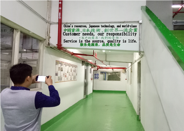
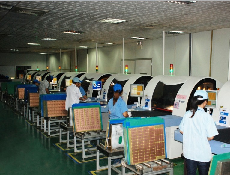
XHPCB was established in 2006, located in ShenZhen of China,occupy 3000 square meters, there are 200 employees,10 engineers.
we engaged in all kinds of PCB design, manufacture services over tenyears, we are a ODM and OEM factory,
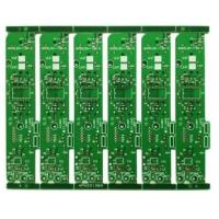
Main for Single-Sided Board, Double-Sided Board, Multilayer Board,Blind via Multilayer board, Buried via multilayer board, and so on.
PCB specification: conductor line/space≧0.01mm, holediameter≧0.2mm, layer quantity≦8
Surface treatment: HASL(lead free) ,HASL(with lead), immersion gold,immersion silver,gold plated ,OSP and so on.
Usage: electronic products, Digital product, LED, auto, communication,Medical,home appliance, computers, consumption goods and so on.
Medical,home appliance, computers, consumption goods and so on.
1: Medical Bluetooth module motherboard
2: Halogen-free FR-4 TG180, inner and outer copper thickness 35um, minimum line width line
spacing 3/3mil, hole ratio 10:1, minimum hole 0.10mm, blind hole
buried hole, immersion gold, red solder resist, white
3: The board thickness is 1.60mm,
4: blind hole, resin plug hole + plating hole
Printed Circuit Boards are 94V0 compliant, and adhere to IPC610
Class 2 international PCB
Standard.
Quantities range from prototype to volume production.
100% E-Test
PCB, FPC process production capability
| Technical ltem | MassProduct | Advanced Technology | |||||
| 2016 | 2017 | 2018 | |||||
| Max.Layer Count | 26L | 36L | 80L | ||||
| Through-hole plate | 2~45L | 2~60L | 2~80L | ||||
| Max.PCBSize(in) | 24*52" | 25*62" | 25*78.75" | ||||
| The layer number of FPC | 1~36L | 1~50L | 1~60L | ||||
| Max.PCBSize(in) | 9.8"*196" | 9.8"*196" | 10"*196"Reel to reel | ||||
| Layeredplatelayer | 2~12L | 2~18L | 2~26L | ||||
| Max.PCBSize(in) | 9"*48" | 9"*52" | 9"*62" | ||||
| Combination of hard and soft layers | 3~26L | 3~30L | 3~50L | ||||
| Interconnect HDI | 5+X+5Interconnect HDI | 7+X+7Interconnect HDI | 8+X+8,Interconnect HDI | ||||
| HDI PCB | 4~45L | 4~60L | 4~80L | ||||
| Interconnect HDI | 3+20+3 | 4+X+4Interconnect HDI | 4+X+4,Interconnect HDI | ||||
| Max.PCBSize(in) | 24"*43" | 24"*49" | 25"*52" | ||||
| Material | FR-4 Rogers | FR-4 Rogers | FR-4 Rogers | ||||
| Base material | Halogenfree,LowDK | Halogenfree,LowDK | Halogenfree,LowDK | ||||
| Build-up Material | FR-4 | FR-4 | FR-4 | ||||
| BOard,Thickness(mm) | Min.12L(mm) | 0.43 | 0.42~8.0mm | 0.38~10.0mm | |||
| Min.16L(mm) | 0.53 | 1.60~8.0mm | 0.45~10.0mm | ||||
| Min.18L(mm) | 0.63 | 2.0~8.0 | 0.51~10.0mm | ||||
| Min.52L(mm) | 0.8 | 2.50~8.0mm | 0.65~10.0mm | ||||
| MAX(mm) | 3.5 | 10.0mm | 10.0mm | ||||
| Min.CoreThickness um(mil) | 254"(10.0) | 254"(10.0) | 0.10~254(10.0mm) | ||||
| Min.Build up Dielectric | 38(1.5) | 32(1.3) | 25(1.0) | ||||
| BaseCopperWeight | Inner Layer | 4/1-8 OZ | 4/1-15 OZ | 4/1-0.30mm | |||
| Out Layer | 4/1-10 OZ | 4/1-15 OZ | 4/1-30 OZ | ||||
| Gold thick | 1~40u" | 1~60u" | 1~120u" | ||||
| Nithick | 76~127u" | 76~200u" | 1~250u" | ||||
| Min.HOle/Land um(mil) | 150/300(6/12) | 100/200(4/8) | 100/200(4/8) | ||||
| Min.Laser via/landum(mil) | 60/170(2.4/6.8) | 50/150(2/6) | 50/150(2/6) | ||||
| Min. IVH,Hole size/landum(mil) | 150/300(6/12) | 100/200(4/8) | 100/200(4/8) | ||||
| DieletricThickness | 38(1.5) | 32(1.3) | 32(1.3) | ||||
| 125(5) | 125(5) | 125(5) | |||||
| SKipvia | Yes | Yes | Yes | ||||
| viaoNhie(laserviaon BuriedPTH) | Yes | Yes | Yes | ||||
| Laser Hole Filling | Yes | Yes | Yes | ||||
| Technicalltem | Mass Product | Advanced Technolgy | |||||
| 2017year | 2018year | 2019year | |||||
| Drill hole depth ratio | ThroughHole | 2017year | .40:1 | .40:1 | |||
| Aspet Ratio | Micro Via | .35:1 | 1.2:1 | 1.2:1 | |||
| Copper Filling Dimple Size um(Mil) | 10(0.4) | 10(0.4) | 10(0.4) | ||||
| Min.LineWidth&space | lnner Layer um(mil) | 45/45(1.8/1.8) | 38/38(1.5/1.5) | 38/38(1.5/1.5) | |||
| Plated Layer um(mil) | 45/45(1.8/1.8) | 38/38(1.5/1.5) | 38/38(1.5/1.5) | ||||
| BGAPitch mm(Mil) | 0.3 | 0.3 | 0.3 | ||||
| Min.PTH Hole ring um(mil) | 75(3mil) | 62.5(2.5mil) | 62.5(2.5mil) | ||||
| Line Width Control | ∠2.5MIL | ±0.50 | ±0.50 | ±0.50 | |||
| 2.5Mil≤L/W∠4mil | ±0.50 | ±0.50 | ±0.50 | ||||
| ≦3mil | ±0.60 | ±0.60 | ±0.60 | ||||
| Laminated structure | Layer by layer | 3+N+3 | 4+N+4 | 5+N+5 | |||
| Sequential Build-up | 20L Any Layer | 36L Any Layer | 52L Any Layer | ||||
| Multi-layer overlay | N+N | N+N | N+N | ||||
| N+X+N | N+X+N | N+X+N | |||||
| sequential Lamination | 2+(N+X+N)+2 | 2+(N+X+N)+2 | 2+(N+X+N)+2 | ||||
| Soft and hard bonding | 2+(N+X+N)+2 | 2+(N+X+N)+2 | 2+(N+X+N)+2 | ||||
| PTH filling process | PTH resin plug hole + plating fill Electroplated hole/copper plug hole | PTH resin plug hole + plating fill Electroplated hole/copper plug hole | PTH resin plug hole + plating fill Electroplated hole/copper plug hole | ||||