

Active Member
|
[China]

Address: Huishang Building, 19-128 Nathan Road, Yau Tsim Sha Tsui, Yau Tsim, Hong Kong
Contact name:Mank.Li

Shenzhen Chaosheng Electronic Technology Co.,Ltd |
|
|
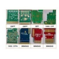
Printed circuit board (pcb) and PCBA product areas
Communication terminals, communication stations, electronic
communications, computers, household appliances, appliances, SD
cards, SG cards, mobile phones, antennas, computers, automobiles,
music equipment, playback equipment, banking equipment, medical
instruments, medical equipment, medical equipment, aerospace,
Aviation, military, LED, OLED, OLCD power control power supply,
industrial power supply, communication power supply, automotive
power supply, office equipment, digital products, computers and
other product applications;
Winding circuit board (fpc) and FPCA product areas
CD, hard disk, printer, fax machine, scanner, sensor, mobile phone,
connector, module, walkie-talkie antenna card, high-end camera,
digital, camera, laser head, CD, medical, instrumentation, drive,
automotive instrumentation, medical instrument , Medical equipment,
banking equipment, industrial instruments, LED strips, military
industry, aviation, aerospace, national defense and other high-tech
products, more than 70% of the products are exported to the
Americas, Europe, Japan, Asia Pacific and other countries and
regions.
PCB, FPC process production capability
| Technical ltem | MassProduct | Advanced Technology | |||||
| 2016 | 2017 | 2018 | |||||
| Max.Layer Count | 26L | 36L | 80L | ||||
| Through-hole plate | 2~45L | 2~60L | 2~80L | ||||
| Max.PCBSize(in) | 24*52" | 25*62" | 25*78.75" | ||||
| The layer number of FPC | 1~36L | 1~50L | 1~60L | ||||
| Max.PCBSize(in) | 9.8"*196" | 9.8"*196" | 10"*196"Reel to reel | ||||
| Layeredplatelayer | 2~12L | 2~18L | 2~26L | ||||
| Max.PCBSize(in) | 9"*48" | 9"*52" | 9"*62" | ||||
| Combination of hard and soft layers | 3~26L | 3~30L | 3~50L | ||||
| Interconnect HDI | 5+X+5Interconnect HDI | 7+X+7Interconnect HDI | 8+X+8,Interconnect HDI | ||||
| HDI PCB | 4~45L | 4~60L | 4~80L | ||||
| Interconnect HDI | 3+20+3 | 4+X+4Interconnect HDI | 4+X+4,Interconnect HDI | ||||
| Max.PCBSize(in) | 24"*43" | 24"*49" | 25"*52" | ||||
| Material | FR-4 Rogers | FR-4 Rogers | FR-4 Rogers | ||||
| Base material | Halogenfree,LowDK | Halogenfree,LowDK | Halogenfree,LowDK | ||||
| Build-up Material | FR-4 | FR-4 | FR-4 | ||||
| BOard,Thickness(mm) | Min.12L(mm) | 0.43 | 0.42~8.0mm | 0.38~10.0mm | |||
| Min.16L(mm) | 0.53 | 1.60~8.0mm | 0.45~10.0mm | ||||
| Min.18L(mm) | 0.63 | 2.0~8.0 | 0.51~10.0mm | ||||
| Min.52L(mm) | 0.8 | 2.50~8.0mm | 0.65~10.0mm | ||||
| MAX(mm) | 3.5 | 10.0mm | 10.0mm | ||||
| Min.CoreThickness um(mil) | 254"(10.0) | 254"(10.0) | 0.10~254(10.0mm) | ||||
| Min.Build up Dielectric | 38(1.5) | 32(1.3) | 25(1.0) | ||||
| BaseCopperWeight | Inner Layer | 4/1-8 OZ | 4/1-15 OZ | 4/1-0.30mm | |||
| Out Layer | 4/1-10 OZ | 4/1-15 OZ | 4/1-30 OZ | ||||
| Gold thick | 1~40u" | 1~60u" | 1~120u" | ||||
| Nithick | 76~127u" | 76~200u" | 1~250u" | ||||
| Min.HOle/Land um(mil) | 150/300(6/12) | 100/200(4/8) | 100/200(4/8) | ||||
| Min.Laser via/landum(mil) | 60/170(2.4/6.8) | 50/150(2/6) | 50/150(2/6) | ||||
| Min. IVH,Hole size/landum(mil) | 150/300(6/12) | 100/200(4/8) | 100/200(4/8) | ||||
| DieletricThickness | 38(1.5) | 32(1.3) | 32(1.3) | ||||
| 125(5) | 125(5) | 125(5) | |||||
| SKipvia | Yes | Yes | Yes | ||||
| viaoNhie(laserviaon BuriedPTH) | Yes | Yes | Yes | ||||
| Laser Hole Filling | Yes | Yes | Yes | ||||
| Technicalltem | Mass Product | Advanced Technolgy | |||||
| 2017year | 2018year | 2019year | |||||
| Drill hole depth ratio | ThroughHole | 2017year | .40:1 | .40:1 | |||
| Aspet Ratio | Micro Via | .35:1 | 1.2:1 | 1.2:1 | |||
| Copper Filling Dimple Size um(Mil) | 10(0.4) | 10(0.4) | 10(0.4) | ||||
| Min.LineWidth&space | lnner Layer um(mil) | 45/45(1.8/1.8) | 38/38(1.5/1.5) | 38/38(1.5/1.5) | |||
| Plated Layer um(mil) | 45/45(1.8/1.8) | 38/38(1.5/1.5) | 38/38(1.5/1.5) | ||||
| BGAPitch mm(Mil) | 0.3 | 0.3 | 0.3 | ||||
| Min.PTH Hole ring um(mil) | 75(3mil) | 62.5(2.5mil) | 62.5(2.5mil) | ||||
| Line Width Control | ∠2.5MIL | ±0.50 | ±0.50 | ±0.50 | |||
| 2.5Mil≤L/W∠4mil | ±0.50 | ±0.50 | ±0.50 | ||||
| ≦3mil | ±0.60 | ±0.60 | ±0.60 | ||||
| Laminated structure | Layer by layer | 3+N+3 | 4+N+4 | 5+N+5 | |||
| Sequential Build-up | 20L Any Layer | 36L Any Layer | 52L Any Layer | ||||
| Multi-layer overlay | N+N | N+N | N+N | ||||
| N+X+N | N+X+N | N+X+N | |||||
| sequential Lamination | 2+(N+X+N)+2 | 2+(N+X+N)+2 | 2+(N+X+N)+2 | ||||
| Soft and hard bonding | 2+(N+X+N)+2 | 2+(N+X+N)+2 | 2+(N+X+N)+2 | ||||
| PTH filling process | PTH resin plug hole + plating fill Electroplated hole/copper plug hole | PTH resin plug hole + plating fill Electroplated hole/copper plug hole | PTH resin plug hole + plating fill Electroplated hole/copper plug hole | ||||
FAQ:
Q: What files do you use in PCB fabrication?
A: Gerber or Eagle, BOM listing, X, Y sitting report, PNP and Components Position
Q: Is it possible you could offer sample?
A: Yes, we can custom you sample to test before mass production
Q: When will I get the quotation after sent Gerber, BOM and test procedure?
A: Within 6-48hours for PCB quotation and around 24-48 hours for PCBA quotation.
Q: According to the difficulty of high-layer boards, How can I know the process of my PCB production?
A: 7-35days for PCB production and components purchasing, and 14-20days for PCB assembly and Testing
Q: How can I make sure the quality of my PCB?
A: We ensure that each piece of PCB, PCBA products work well before shipping. We'll test all of them according to your test procedure.
We are the manufacturer with ISO standard certification in
GuangDong China that specialize in producing all kinds of PCB(print
Circuit Board) with reliable quality. All products are selled by
Factory Price.
the price is variable according to the complexity of your design.
You can send your inquiry with required documents( such as Gerber
File, Protel or DXP format File, Cadence format File, PADS format
file). We will reviews your files and reply in a few hours with
competitive price and valuable comments & suggestions.
We also have PCB SMT Production Line and can provide SMT service.
If you have similar requirements, please contact us.
| Specifications | ||
| 1 | NO. LAYER | 1-32(Batch Process) 1-32 (Sample Board) |
| 2 | FINISHED BOARD SIZE (MAX) | 520mm X 1040mm |
| 3 | BOARD THICKNESS (MAX) | 5.0mm |
| 4 | BOARD THICKNESS (MIN) | 0.50mm |
| 5 | DRILLED HOLE DIAMETER (MIN) | 0.25mm |
| 6 | DIELECTRIC MATERIAL (MIN) | CEM-3 FR4(130C Tg) Rogcrs4003 FR4(140C Tg) FR4(150-170C Tg) |
| 7 | HOLE DIAMETER TOLERANCE (PTH) | +/-2mils(Batch Process) |
| 8 | HOLE DIAMETER TOLERANCE (NPTH) | +/-2mils(Batch Process) |
| 9 | LAYERLINE WIDTH/SPACING (MIN) | H/H Oz is 3mil/3mil 1/1 oz is 3mil/3mil 2/2 oz is 5mil/5mil |
| 10 | SOLDER MASK THICKNESS (MIN) | 10 Um |
| 11 | IMPEDANCE TOLERANCE (MIN) | +/-10% |
| 12 | Surface Processing | 1. HASL 3. Deposited Nickel/Gold |
| 13 | THERMAL STRESS TEST | 288 Centigrade,10 sec One Shot |
| 14 | FLAMMABILITY | 94V-0 |


