
|
|
[China]

Trade Verify
Contact name:Rain Kong

Guangzhou Kaijin Precision Manufaturing Co., Ltd. |
|
Verified Suppliers
|
|
|
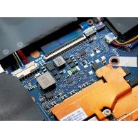
PCB Prototype is a reliable manufacturer that specializes in 4 layer PCB prototype and PCB board making. We offer a comprehensive range of PCB assembly services that guarantee quality levels with stringent standards and accuracy. Our PCB prototype products are created with advanced techniques like Flying Probe Test and E-test to ensure that all the components are tested with precision and accuracy. In addition, all our PCB prototypes are manufactured with white silkscreen and precision measurements of 0.2mm for both the minimum hole size and minimum space, as well as minimum trace width. Our professional team is committed to delivering the highest quality of PCB prototypes that meet your individual needs and requirements.
| Parameter | Value |
|---|---|
| Solder Mask | Green |
| PCB QC | Flying Probe Test, E-test |
| Layer | 2 |
| Minimum Hole Size | 0.2mm |
| Board Thickness | 1.6mm |
| Material | FR4 |
| PCBA QC | X-ray, AOI Inspection, Functional Test |
| Minimum Trace Width | 0.2mm |
| Minimum Space | 0.2mm |
| Minimum Annular Ring | 0.1mm |
PCB Prototype is a type of printed circuit board that is made of a flexible material, typically FR4, with a thickness of 1.6mm. It is designed to handle the complex circuits and components that are too dense for regular PCBs. The PCB Prototype has a solder mask of green that allows for accurate and precise soldering of the components. The minimum trace width of 0.2mm allows for the most intricate circuits and components to be attached. Additionally, the PCB Prototype has white silkscreen printing that allows for the easy identification of components and circuits.
The PCB Prototype is suitable for a wide range of applications, from prototyping to production. It is often used in the development of complex technologies such as flexible displays, wearables, and medical devices. It is also used in the production of consumer electronics such as smartphones, tablets, and game consoles. The PCB Prototype is also perfect for prototyping four-layer PCBs, which require a higher level of precision than regular PCBs.
We provide AOI Inspection, fr4 double sided pcb, and low cost pcb prototype services.
Our pcb prototype is customized with minSpace: 0.2mm, minTraceWidth: 0.2mm, solderMask: Green, layer: 2, and minAnnularRing: 0.1mm.
We provide comprehensive technical support and service for PCB Prototype products.
If you need any help with your PCB Prototype product, please do not hesitate to contact us.
PCB Prototypes must be packaged and shipped properly to ensure that they are protected from damage. The following are the steps for packaging and shipping PCB prototypes:
A: A PCB Prototype is a physical representation of a printed circuit board which is used to test the design and functionality of an electronic device before it is manufactured.
A: There are several types of PCB Prototypes available, including single-sided, double-sided, and multilayer printed circuit boards.
A: PCB Prototypes provide an efficient way to test and troubleshoot a design prior to manufacturing, allowing manufacturers to identify and fix any issues before committing to a large-scale production run.
A: The time it takes to create a PCB Prototype depends on the complexity of the design and the type of PCB being used. Generally, it can take anywhere from a few days to a few weeks.
A: Yes. PCB Prototypes are designed to be as reliable as the final product. However, it is important to test the prototype thoroughly to ensure that it meets the specified requirements.


