
|
|
[China]

Trade Verify
Contact name:Rain Kong

Guangzhou Kaijin Precision Manufaturing Co., Ltd. |
|
Verified Suppliers
|
|
|
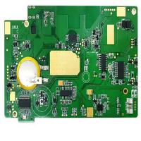
| Product name | High-quality PCB board Custom Android motherboard Industrial control board |
| Disposition | 2G RAM,16GeMMC,4G,wifi,BT,RJ 45 |
| Application Scope | This product is intelligent Android motherboard, suitable for face recognitionterminal, face payment terminal and security |
| Main board size | 68.4*115.0*1.2mmMain |
| board fixing hole | D2.1* 4 |
Product characteristics
Memory :2GB LPDDR3+16GB eMMC(default)4GB LPDDR3+32GB
eMMC(optional)4G LTE: Support 3GPP R8 Cat6 and
Cat4,VoLTEWLAN:2.4G/5GHz,IEEE802.11a/b/g/n/ac
GNSS GPS/GLONASS/BeiDou个
Display output: maximum support for MIPI-1280X800,
LVDS-1920X1080EDP-1920X1080,HDMI-1080P output (Main panel LVDS
signal output, Slavepanel is MIPI signal. if required, other
interfaces through the transfer board).RTC4
Audio output:1*2W/8R or 2*1.5W/8R
5*USB2.0,1*10/100M RJ45,1RS-232,2*UART(3V3)红Support Android 7/9
system customization, provide system APIlinterface code.perfect
customer upper-level APP development4Voltage DC input: DC +12V,
rated power <18WOperating temperature: -10°C~+ 45C, humidity:
10%~90%
The PCB manufacturing process typically involves the following steps:
Design: The circuit design is created using specialized software, which generates a file that contains information about the layout, component placement, and connections.
PCB Layout: The PCB layout is created from the design file, and includes the placement of components, routing of connections, and the creation of copper traces and pads.
PCB Imaging: The PCB layout is transferred onto a photosensitive material using a process called imaging. This creates a pattern that is used to etch the copper layer.
Etching: The copper layer is etched using chemicals, which removes the copper from the areas that are not covered by the photosensitive material.
Drilling: Holes are drilled into the PCB to allow for component placement and connections.
Plating: A thin layer of metal (usually copper) is plated onto the holes and surface of the PCB to improve conductivity.
Solder Mask: A layer of solder mask is applied to protect the copper traces and pads from oxidation and damage during the soldering process.
Silkscreen: A layer of silkscreen is added to label the components and provide other information.
Testing: The finished PCB is tested to ensure that it functions correctly and meets the required specifications.


Why did you choose us?
1. Experienced
Focus on PCBA electronics manufacturing for 8 years
Best partner for listed companies
Serving more than 60 European and American enterprises
Helped customers solve design problems more than 500 times
Help customers solve MP problems more than 800 times.
Help customers improve test reliability by more than 1000 times
2. Quality control
ISO9001:2015 quality management system certification
ISO13485 quality management system certification
IATF16949
LE2
Traceability system
Fully automated FCT testing
3. Quick response
Quick response principle within 1 hour
7 days * 24 hours
Team accountability
Sales staff with bachelor degree or above


