

Active Member
|
Address: 810-818#, Yufeng building,6-9# Jinhai road, Yantian community,Xixiang street,Bao'an district, Shenzhen city
Contact name:

MOKO TECHNOLOGY LTD |
|
|
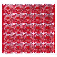
Custom FR-4 Red Solder Mask Double Side PCB Board 4 Layers Fabrication
4 Layers PCB
1.20mm Finish Thickness
1OZ finish Copper
Lead Free Hasl finish
Red Solder Mask
6/6 mil Min track/spacing
0.25mm hole size
V-Cut outline
Brand:China PCB Fabrication
PCB Technical Capacity
1. Files: Gerber, Protel, Powerpcb, Autocad, Orcad, etc
2. Material: FR-4, Hi-Tg FR-4, Lead free Materials (RoHS Compliant) , CEM-3, CEM-1,
Aluminium, High frequency Material (Rogers, Teflon, Taconic)
3. Layer No.: 1 - 28 Layers
4. Board thickness: 0.0075"(0.2mm)-0.125"(3.2mm)
5. Board Thickness: Tolerance: ±10%
6. Copper thickness: 0.5OZ - 4OZ
7. Impedance Control: ±10%
8. Warpage: 0.075%-1.5%
9. Peelable: 0.012"(0.3mm)-0.02’(0.5mm)
10. Min Trace Width (a): 0.005"(0.125mm)
11. Min Space Width (b): 0.005"(0.125mm)
12. Min Annular Ring: 0.005"(0.125mm)
13. SMD Pitch (a): 0.012"(0.3mm)
14. pcb with green solder mask and LF-FREE surface finishing BGA Pitch (b): 0.027"(0.675mm)
15. Regesiter tolerance: 0.05mm
16. Min Solder Mask Dam (a): 0.005"(0.125mm)
17. Soldermask Clearance (b): 0.005"(0.125mm)
18. Min SMT Pad spacing (c): 0.004"(0.1mm)
19. Solder Mask Thickness: 0.0007"(0.018mm)
20. Hole size: 0.01"(0.25mm)-- 0.257"(6.5mm)
21. Hole Size Tolerance: ±0.003"(±0.0762mm)
22. Aspect Ratio: 6:01:00
23. Hole Registration: 0.004"(0.1mm)
24. HASL: 2.5um
25. Lead free HASL: 2.5um
26. Immersion Gold: Nickel :3-7um Au:1-3u''
27. OSP: 0.2-0.5um
28. Panel Outline Tolerance: ±0.004''(±0.1mm)
29. Beveling: 30°45°
30. V-cut: 15° 30° 45° 60°
31. Surface finish: HAL, HASL Lead Free, Immersion gold, Gold plating, Gold finger, immersion
silver, immersion Tin, OSP, Carbon ink,
32. Certificate : ROHS ISO9001:2000 TS16949 SGS UL
33. Special requirements: Buried and blind vias, Impedance control, via plug, BGA soldering
and gold finger.


