

Active Member
|
[China]

Address: 4113-4116# A Area, HSST PARK, BAO'AN District, Shenzhen, China
Contact name:Wendy

Abis Circuits Co., Ltd. |
|
|
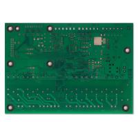
OEM 2 Layer Fr4 PCB Circuit Board Green Ink Double Sided PCB Fabrication
About us
Abis Circuits Co. Ltd, established in 2006, Located in Shenzhen, our company has about 1100 workers and two PCB workshops with about 50000 square meters.
Our products are mostly used in the field of Industrial Control, Telecommunication, Automotive products, Medical, Consumer, Security, and others.
Our perfect management, advanced equipment, and professional staffs are the keys for us to fight to win more market shares with other competitors. Customer satisfaction and support are what we have been strived for.
We Can Offer :
1. PCB Manufacture: PCB file or Gerber file needed
2. PCB PCBA SMD SMT Assembly: Gerber File and Bom list needed
3. Reverse Engineering - PCB Copy, PCB Clone, IC Decode
4. Professtional Components Procurement
5. PCB PCBA Finished Product Test
6. PCB And PCBA Mass-Production
Factory Overview
| Shenzhen | Jiangxi | |
| Area | 10,000 Square meters | 60000 Square meters |
| Employees | 300 | 900 |
| Quality | 20 | 60 |
Administration | 5 | 10 |
| Engnieering | 20 | 90 |
Over Sales | 10 | 20 |
| Process Capability | ||||||||||||||
| Material Type: FR4/Aluminum/Ceramic/CEM-1/Copper/polytef | Cooper thickness: 0.5-12OZ | |||||||||||||
| Board Thickness: 0.25-6.0mm | Min hole size: 0.2mm( finished hole size) | |||||||||||||
| Min Line Width/spacing:0.08mm | Drilling accuracy:+/-0.05 | |||||||||||||
| Max working size:520*620mm(21.25x24.5inch) | Min Inner layer thickness:0.1mm | |||||||||||||
| Min thickness Board for HAL surface finished:0.4mm | Certificate: Rohs, Iso9001, UL(in certification) | |||||||||||||
| Min thickness 4 layer: 0.4mm | Min thickness 6 layer:0.6mm | |||||||||||||
| Min/Max layer count : 1/20 | Lamination evenness :+/-0.05mm | |||||||||||||
| Min SMD Pitch : 0.125mm | Min Dam Between Fine Pitch: >0.1mm | |||||||||||||
| Layer to Layer registration:<0.1mm | Impedance control:+/-5% | |||||||||||||
| Differential impedance:+/-10% | Board bow/twist tolerance:<0.7% | |||||||||||||
| Plating spect ratio: <8:1 | Plating COV: <10% | |||||||||||||
| Surface Finished: LF-HASL ,Immersion Gold/Tin/Silver ./Plating Gold/OSP, | PTH backlight : 9-9.5 level | |||||||||||||
| Solder Mask:Green , Red, Blue,White, Black,Yellow. | Plating extensibility:>15% | |||||||||||||
Lead Time
| Category | Q/T Lead time | Standard Lead Time | Mass Production | |||
| 2 Layers | 24hrs | 3-4 working days | 8-15 working days | |||
| 4 Layers | 48hrs | 3-5 working days | 10-15 working days | |||
| 6 Layers | 72hrs | 3-6 working days | 10-15 working days | |||
| 8 Layers | 96hrs | 3-7 working days | 14-18 working days | |||
| 10 Layers | 120hrs | 3-8 working days | 14-18 working days | |||
| 12 Layers | 120hrs | 3-9 working days | 20-26 working days | |||
| 14 Layers | 144hrs | 3-10 working days | 20-26 working days | |||
| 16-20 Layers | Depends on the specific requirements | |||||
| 20+ Layers | Depends on the specific requirements | |||||
Packaging & Delivery
ABIS CIRCUITS Company is not only trying to give customers a good product, but also pay attention to offering a complete and safe package. Also, we prepare some personalized services for all the orders.
-Common packaging:
Certificate

PCB Manufacturing Process
- The process starts with designing Layout of the PCB using any PCB designing software / CAD Tool (Proteus, Eagle, Or CAD).
- All rest of the steps are of Manufacturing Process of a Rigid Printed Circuit Board is same as Single Sided PCB or Double Sided PCB or Multi-layer PCB.

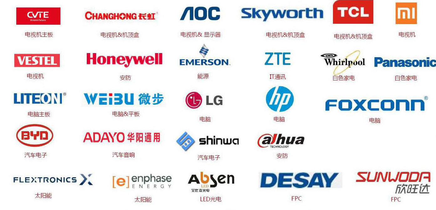
Abis honor customer
FAQ
Q1:What service do you have?
A1: We provide turnkey solution including RD, PCB fabrication, SMT, final assembly,testing and other value-added service.
Q2:What are the main products of your PCB/PCBA services?
A2:Our PCB/PCBA services are mainly for the industries including Medical, Automotive, Energy,Metering/Measurements. Consumer Electronics.
Q3:How can we ensure our information should not let third party to see our design?
A3: We are wiling to sign NDA effect by customer side locallaw and promising to keep customers datain highconfidential level.
Q4:What does Parason need for a customized PCB order?
A4:When you place a PCB order, the customers need to provide Gerber file.If you do not have the fileinthe correct format, you can send all the details related to the products.
Q5:What will be needed for a customized PCBA order?
A5: When you place a PCBA order, you need to provide Gerber or pcb file and the BOM list to us.
Q6:Do you have an minimum order quantity?
A6:We accept order with as low as a quantity of 1 (piece or panel)


