

Active Member
|
[China]

Address: 4113-4116# A Area, HSST PARK, BAO'AN District, Shenzhen, China
Contact name:Wendy

Abis Circuits Co., Ltd. |

|
|
FR4 CEM1 CTI600 HASL Prototype PCB Board 1.2mm 6 Layer PCB Board
| Item | Spec |
| Layers | 1~20 |
| Board Thickness | 0.1mm-8.0mm |
| Material | FR-4, CEM-1/CEM-3, PI, High Tg, Rogers, PTEF, Alu/Cu Base, etc |
| Max Panel Size | 600mm×1200mm |
| Min Hole Size | 0.1mm |
| Min Line Width/Space | 3mil(0.075mm) |
| Board Outline Tolerance | 士0.10mm |
| Insulation Layer Thickness | 0.075mm--5.00mm |
| Out Layer Copper Thickness | 18um--350um |
| Drilling Hole (Mechanical) | 17um--175um |
| Finish Hole (Mechanical) | 0.10mm--6.30mm |
| Diameter Tolerance (Mechanical) | 0.05mm |
| Registration (Mechanical) | 0.075mm |
| Aspect Ratio | 16:01 |
| Solder Mask Type | LPI |
| SMT Mini. Solder Mask Width | 0.075mm |
| Mini. Solder Mask Clearance | 0.05mm |
| Plug Hole Diameter | 0.25mm--0.60mm |
| Impedance Control Tolerance | 士10% |
| Surface finish | ENIG, OSP, HASL, Chem. Tin/Sn, Flash Gold |
| Soldermask | Green/Yellow/Black/White/Red/Blue |
| Silkscreen | Red/Yellow/Black/White |
| Certificate | UL, ISO 9001, ISO14001, IATF16949 |
| Special Request | Blind hole, Gold finger, BGA, Carbon ink, peekable mask, VIP process, Edge plating, Half holes |
| Material Suppilers | Shengyi, ITEQ, Taiyo, etc. |
| Common Package | Vacuum+Carton |
PCB Lead Time
| Category | Q/T Lead time | Standard Lead Time | Mass Production | |||
| Double Sided | 24hrs | 3-4 working days | 8-15 working days | |||
| 4 Layers | 48hrs | 3-5 working days | 10-15 working days | |||
| 6 Layers | 72hrs | 3-6 working days | 10-15 working days | |||
| 8 Layers | 96hrs | 3-7 working days | 14-18 working days | |||
| 10 Layers | 120hrs | 3-8 working days | 14-18 working days | |||
| 12 Layers | 120hrs | 3-9 working days | 20-26 working days | |||
| 14 Layers | 144hrs | 3-10 working days | 20-26 working days | |||
| 16-20 Layers | Depends on the specific requirements | |||||
| 20+ Layers | Depends on the specific requirements | |||||
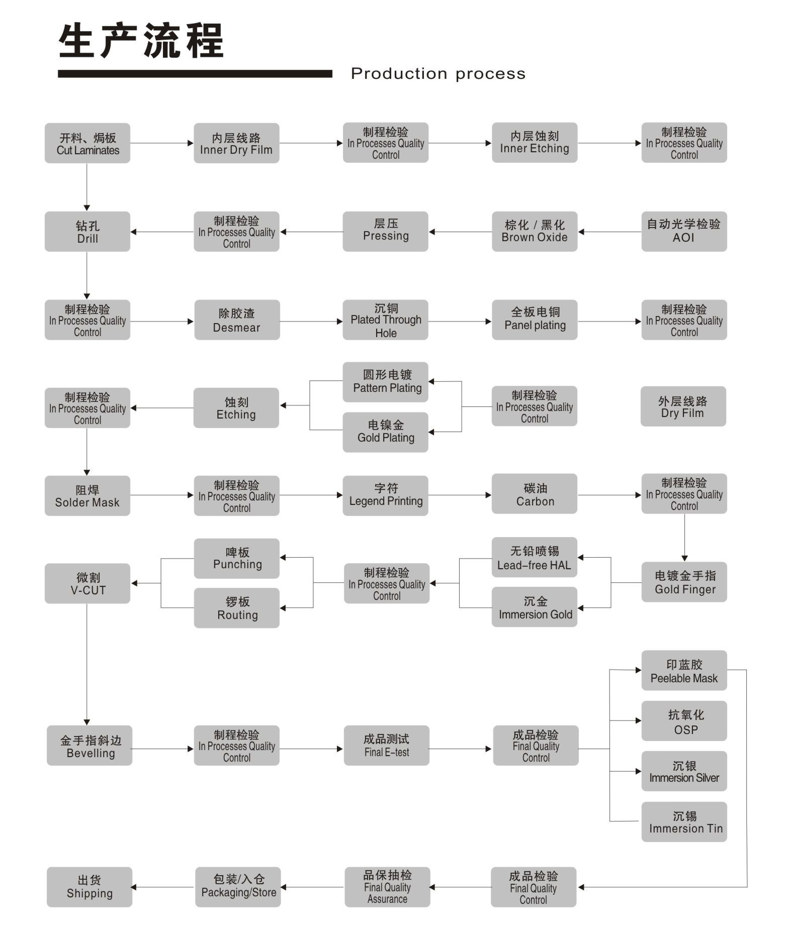
How ABIS Working Out the Manufacturing Issues in FR4 PCB?
-Hole Preparation
Removing debris carefully & adjusting drill machine parameters: before plating through with copper, abis pays high attention to all holes on an fr4 pcb treated to remove debris, surface irregularities, and epoxy smear, the clean holes ensure the plating successfully adheres to the hole walls. also, early in the process, drill machine parameters are adjusted accurately.
- Surface Preparation
Deburring carefully: our experienced tech workers will be aware ahead of time that the only way to avoid a bad outcome is to anticipate the need for special handling and to take the appropriate steps to be sure that the process is done carefully and correctly.
-Thermal Expansion Rates
Accustomed to dealing with the various materials, abis will be able to analyze the combination to be sure that it is appropriate. then keeping the long-term reliability of the cte (coefficient of thermal expansion), with the lower cte, the less likely the plated through holes are to fail from repeated flexing of the copper which forms the internal layer interconnections.
-Scaling
Abis control the circuitry is scaled-up by known percentages in anticipation of this loss so that the layers will return to their as-designed dimensions after the lamination cycle is complete. also, using the laminate manufacturer’s baseline scaling recommendations in combination with in-house statistical process control data, to dial-in scale factors that will be consistent over time within that particular manufacturing environment.
-Machining
When the time comes to build your pcb, abis be sure that you choose has the right equipment and experience to produce it correctly on the first try.


Packaging & Delivery
ABIS CIRCUITS Company is not only trying to give customers a good product, but also pay attention to offering a complete and safe package. Also, we prepare some personalized services for all the orders.
-Common packaging:

-Delivery Tips:

Business Terms
-Accepted Delivery Terms
FOB, CIF, EXW, FCA, CPT, DDP, DDU, Express Delivery, DAF
--Accepted Payment Currency
USD, EUR, CNY.
-Accepted Payment Type
T/T, PayPal, Western Union.
Quotation from ABIS
To ensure an accurate quote, be sure to include the following information for your project:
Your custom quote will be delivered in just 2-24 hours, depending on the design complexity.
ABIS cares every your order even 1 piece


