

Active Member
|
[China]

Address: 4113-4116# A Area, HSST PARK, BAO'AN District, Shenzhen, China
Contact name:Wendy

Abis Circuits Co., Ltd. |

|
|
2 Oz High Density HDI PCB Board 4 Layer Printed Circuit Boards With Blue Solder Mask PCB Manufacturing
The 1.6mm HDI PCB Circuit Board is 4 Layers, and it was made with FR - 4 board material, with 2 Oz / 70µm copper thickness.
Also, the board size of this PCB Circuit Board is customized, with blue solder mask and HASL Lead Free surface treatment.
Detail Specifications
| Layers | 4 |
| Material | FR-4 |
| Board Thickness | 1.6mm |
| Copper Thickness | 2oz/70um |
| Surface Treatment | HASL Lead Free |
| Soldmask & Silkscreen | Blue&White |
| Quality Standard | IPC Class 2, 100% E-testing |
| Certificates | ISO14001, ISO9001, UL, cUL, TS16949 |
PCB Capacity
| Layers | 1~20 |
| Board Thickness | 0.1mm-8.0mm |
| Material | FR4, CEM-1/CEM-3, PI, High Tg, Rogers, PTEF, Alu/Cu Base, etc |
| Max Panel Size | 600mm×1200mm |
| Min Hole Size | 0.1mm |
| Min Line Width/Space | 3mil(0.075mm) |
| Board Outline Tolerance | 0.10mm |
| Insulation Layer Thickness | 0.075mm--5.00mm |
| Out Layer Copper Thickness | 18um--350um |
| Drilling Hole (Mechanical) | 17um--175um |
| Finish Hole (Mechanical) | 0.10mm--6.30mm |
| Diameter Tolerance (Mechanical) | 0.05mm |
| Registration (Mechanical) | 0.075mm |
| Aspect Ratio | 16:01 |
| Solder Mask Type | LPI |
| SMT Mini. Solder Mask Width | 0.075mm |
| Mini. Solder Mask Clearance | 0.05mm |
| Plug Hole Diameter | 0.25mm--0.60mm |
| Impedance Control Tolerance | 10% |
| Surface finish | ENIG, OSP, HASL, Chem. Tin/Sn, Flash Gold |
| Soldermask | Green/Yellow/Black/White/Red/Blue |
| Silkscreen | Red/Yellow/Black/White |
| Certificate | UL, ISO 9001, ISO14001, IATF16949 |
| Special Request | Blind hole, Gold finger, BGA, Carbon ink, peelable mask, VIP process, Edge plating, Half holes |
| Material Suppliers | Shengyi, ITEQ, Taiyo, etc. |
| Common Package | Vacuum+Carton |
PCBA Capacity
| Capacity | |
| Single and double-sided SMT/PTH | Yes |
| Large parts on both sides, BGA on both sides | Yes |
| Smallest Chips size | 0201 |
| Min BGA and Micro BGA pitch and ball counts | 0.008 in. (0.2mm) pitch, ball count greater than 1000 |
| Min Leaded parts pitch | 0.008 in. (0.2 mm) |
| Max Parts size assembly by machine | 2.2 in. x 2.2 in. x 0.6 in. |
| Assembly surface mount connectors | Yes |
| Odd form parts: | Yes, Assembly by hands |
| LED | |
| Resistor and capacitor networks | |
| Electrolytic capacitors | |
| Variable resistors and capacitors (pots) | |
| Sockets | |
| Reflow soldering | Yes |
| Max PCB size | 14.5 in. x 19.5 in. |
| Min PCB Thickness | 0.2 |
| Fiducial Marks | Preferred but not required |
| PCB Finish: | 1. SMOBC/HASL |
| 2. Electrolytic gold | |
| 3. Electroless gold | |
| 4. Electroless silver | |
| 5. Immersion gold | |
| 6. Immersion tin | |
| 7. OSP | |
| PCB Shape | Any |
| Panelized PCB | 1. Tab routed |
| 2. Breakaway tabs | |
| 3. V-Scored | |
| 4. Routed+ V scored | |
| Inspection | 1. X-ray analysis |
| 2. Microscope to 20X | |
| Rework | 1. BGA removal and replacement station |
| 2. SMT IR rework station | |
| 3. Thru-hole rework station | |
| Firmware | Provide programming firmware files,Firmware + software installation instructions |
| Function test | Level of testing required along with test instructions |
| PCB file: | PCB Altium/Gerber/Eagle files (Including specs such as thickness, copper thickness, solder mask colour, finish, etc) |
Lead Time (Peak production time might deffer, please RFQ)
| Category | Q/T Lead time | Standard Lead Time | Mass Production | |||
| 2 Layers | 24hrs | 3-4 working days | 8-15 working days | |||
| 4 Layers | 48hrs | 3-5 working days | 10-15 working days | |||
| 6 Layers | 72hrs | 3-6 working days | 10-15 working days | |||
| 8 Layers | 96hrs | 3-7 working days | 14-18 working days | |||
| 10 Layers | 120hrs | 3-8 working days | 14-18 working days | |||
| 12 Layers | 120hrs | 3-9 working days | 20-26 working days | |||
| 14 Layers | 144hrs | 3-10 working days | 20-26 working days | |||
| 16-20 Layers | Depends on the specific requirements | |||||
| 20+ Layers | Depends on the specific requirements | |||||
About us
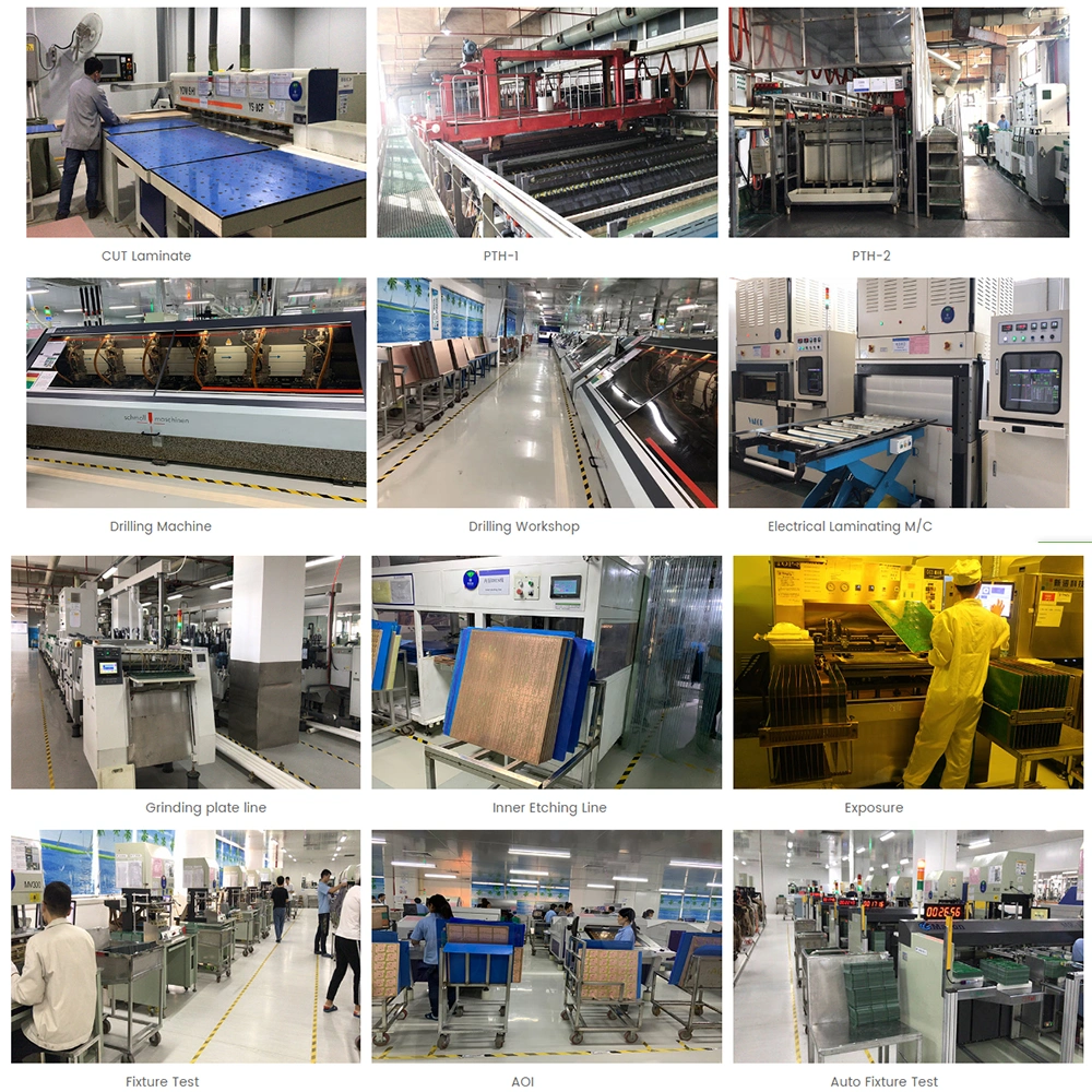
ABIS Circuits Co., Ltd established in 2006, Located in Shenzhen, our company has about 1100 workers and two PCB workshops with about 50000 square meters.
Factory:
What ABIS Circuit can do for you:
PCB manufacturing (prototype, small to medium, mass production)
Quotation of ABIS
To ensure an accurate quote, be sure to include the following information for your project:
Your custom quote will be delivered in just 2-24 hours, depending on the design complexity.
North America
Factory overview
FAQ
1. What kinds of boards can ABIS process?
Common FR4, high-TG and halogen-free boards, Rogers, Arlon, Telfon, aluminum/copper-based boards, PI, etc.
2. What data are needed for PCB production?
PCB Gerber files with RS-274-X format.
3. What’s the typical process flow for multi-layer PCB?
Material cutting → Inner dry film → inner etching → Inner AOI → Multi-bond→ Layer stack up Pressing → Drilling → PTH → Panel Plating → Outer Dry Film → Pattern Plating → Outer etching → Outer AOI → Solder Mask → Component Mark → Surface finish → Routing → E/T → Visual Inspection.
4. How many types of surface finish ABIS can do?
the leader has the full series of surface finish, such as: ENIG, OSP, LF-HASL, gold plating (soft/hard), immersion silver, Tin, silver plating, immersion tin plating, carbon ink and etc. .. OSP, ENIG, OSP + ENIG commonly used on the HDI, we usually recommend that you use a client or OSP OSP + ENIG if BGA PAD size less than 0.3 mm.
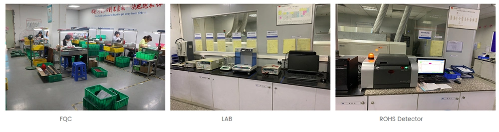
5. How do ABIS ensure quality?
Our high quality standard is achieved with the following.
1.1 The process is strictly controlled under ISO 9001:2008
standards.
1.2 Extensive use of software in managing the production process
1.3 State-of-art testing equipments and tools. E.g. Flying
Probe,e-Testing, X-ray Inspection, AOI (Automated Optical
Inspector) .
1.4.Dedicated quality assurance team with failure case analysis
process
ABIS cares every your order even 1 piece


