
|
|
[China]

Trade Verify
Address: Building C5/B6, Yanchuan North Industrial Park, Yanluo Street, Baoan District, Shenzhen, China
Contact name:Rachel

Shenzhen Benqiang Circuits Co,Ltd. |
|
Verified Suppliers
|
|
|
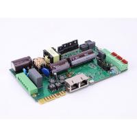
High Reliability Communication PCB Assembly with Immersion Gold Process
Communication PCB Assembly is a vital component in the production of communication equipment. It is responsible for connecting the different parts of the communication board and ensuring their proper functioning. With a variety of surface finishes and advanced PCB gold process, our Communication PCB Assembly guarantees high-quality performance and reliable communication connections.
Our Communication PCB Assembly is a 6-layer printed circuit board (PCB) that is designed specifically for communication equipment. It is available in different surface finishes including HASL, ENIG, OSP, and Immersion Silver, allowing you to choose the most suitable finish for your specific needs. The PCB layers are carefully designed to provide optimal performance and durability, making it ideal for use in communication devices.
The surface finish of a PCB is crucial in determining its performance, reliability, and durability. Our Communication PCB Assembly offers a variety of surface finishes to choose from, including:
Each of these surface finishes has its own unique benefits and is suitable for different applications. Our team of experts can help you choose the most suitable surface finish for your specific communication equipment requirements.
Our Communication PCB Assembly is a 6-layer PCB that is designed to provide high-performance and reliable connections for communication equipment. The multiple layers allow for complex circuitry and reduce the overall size of the PCB, making it more compact and efficient.
The minimum hole diameter of our Communication PCB Assembly is 0.2mm, ensuring precise and accurate connections for your communication equipment. This small diameter allows for more components to be placed on the PCB, making it more versatile and efficient.
Our Communication PCB Assembly undergoes a 100% E-test to ensure its functionality and reliability. This test involves checking each connection and component on the PCB to ensure that they are functioning as intended. This rigorous testing process guarantees that our PCB Assembly meets the highest quality standards and can provide stable and efficient communication connections.
In addition to the surface finish options, our Communication PCB Assembly also offers an advanced PCB gold process known as Immersion Gold. This process involves coating the PCB with a thin layer of gold, which provides excellent conductivity and corrosion resistance. This makes our PCB Assembly ideal for use in communication equipment where reliable and stable connections are crucial.
Communication Telecom PCB Assembly, Communication Board Mount Assembly, and PCB Assembly for Communication Equipment – whatever your communication equipment needs, our Communication PCB Assembly can provide reliable and high-performance connections. With advanced surface finishes, multiple layers, small hole diameter, thorough testing, and advanced PCB gold process, our PCB Assembly is the perfect choice for your communication equipment. Contact us today to learn more about our Communication PCB Assembly and how it can benefit your business.
| Feature | High Reliability And Precision |
|---|---|
| Material Of Pcb | FR-4 |
| Pcba Product Name | 4G Communication/Network Switch |
| Test | 100% E-Test |
| Project | Processing Of Incoming Materials |
| Pcb Material | FR-4 |
| Surface Finish | HASL, ENIG, OSP, Immersion Silver |
| Item | PCB Assembly |
| Pcb Glod Process | Immersion Gold |
| Pcb Request | Gerber&BOM |
Keywords: Communication Device PCB Assembly, Communication Device PCB Assembly, Communication Printed Circuit Board Assembly
The Communication PCB Assembly is an essential component in the field of telecommunication equipment. It plays a crucial role in the efficient communication and transfer of data in various communication systems. This PCB assembly is designed specifically for communication applications and is made of high-quality FR-4 material, ensuring reliable connection and stable performance.
The Communication PCB Assembly is widely used in different communication systems, such as mobile phones, routers, satellites, and other telecommunication devices. It is also commonly used in communication motherboard assembly, where it serves as the main circuit board for the entire system. In this assembly, the PCB is responsible for connecting and controlling all the high-performance components, ensuring smooth and efficient communication.
The Communication PCB Assembly is made of FR-4 material, which is a type of flame-retardant glass fiber epoxy laminate. This material is widely used in the electronics industry due to its high strength, heat resistance, and excellent electrical insulation properties. The PCB gold process used in this assembly is immersion gold, which provides a smooth and reliable surface for the mounting of components and ensures a stable and durable connection.
The processing of incoming materials is a crucial step in the production of Communication PCB Assembly. The FR-4 material is carefully inspected and tested to ensure its quality before being used in the assembly. The high-quality PCB gold process is also strictly monitored to ensure its effectiveness in providing a reliable surface for the components. This meticulous process guarantees that the final product meets the highest standards of quality and performance.
The Communication PCB Assembly is designed with advanced technology and high-density circuit design. This allows for a more compact and efficient layout of components, making it suitable for use in smaller telecommunication devices. The high-density circuit design also ensures the efficient transfer of data and signals, making it an ideal choice for high-speed communication systems.
One of the main advantages of the Communication PCB Assembly is its ability to provide a stable and durable connection in various communication systems. Its high-performance components and advanced technology make it a reliable choice for efficient communication. The use of FR-4 material and immersion gold process also ensures the longevity and durability of the assembly, making it a cost-effective option for telecommunication equipment manufacturers.
The Communication PCB Assembly is a vital component in the field of telecommunication equipment. Its use of high-quality FR-4 material, immersion gold process, and advanced technology makes it a reliable and efficient choice for communication systems. With its high-speed data transfer, high-density circuit design, and stable performance, this PCB assembly is essential for achieving efficient communication in today's fast-paced world.
Item: PCB Assembly
PCB Application: AI Android Smart Module
Minimum Hole Diameter: 0.2mm
PCB Layers: 6 Layers
PCB Request: Gerber & BOM
At Electronics Assembly, we specialize in providing top-quality Communication PCB Assembly services for our clients. Our skilled technicians have years of experience in the industry, and are dedicated to delivering reliable and efficient solutions for your communication needs.
Our Communication Board Mount Assembly services are designed to meet the specific requirements of the AI Android Smart Module. We understand the importance of precision and accuracy in this field, and thus we offer a minimum hole diameter of 0.2mm to ensure optimal performance.
Our PCB Assembly services also come with a 6 Layers option, providing you with the flexibility and functionality you need for your communication network. We utilize Gerber & BOM files to ensure seamless integration and compatibility with your existing systems.
When it comes to Communication Network Assembly Board, we are your go-to partner for all your customization needs. Our team is committed to delivering high-quality products and services, and we strive to exceed your expectations every time.
Our Communication PCB Assembly products are carefully packaged to ensure safe delivery to our customers. Each package is designed to protect the delicate components and prevent any damage during shipping.
The Communication PCB Assembly is first placed in an anti-static bag to prevent any electrostatic discharge during handling and shipping. It is then placed in a sturdy cardboard box with foam inserts to provide additional protection against any external impact. The box is sealed with high-quality packaging tape to ensure the contents remain secure during transit.
For bulk orders, the Communication PCB Assembly is packaged in a larger box with added cushioning material to prevent any movement and potential damage during shipping.
We offer various shipping options to meet the specific needs of our customers. Our standard shipping method is via reputable courier services, which provide reliable and timely delivery. For urgent orders, we also offer expedited shipping options such as air freight or overnight delivery.
Our team carefully tracks each shipment to ensure timely delivery and provides customers with tracking information to monitor the progress of their order.
For international orders, we comply with all necessary customs and export regulations to ensure smooth delivery without any delays or issues.
At Communication PCB Assembly, we strive to provide our customers with a hassle-free and seamless shipping experience. Our packaging and shipping processes are designed to deliver our products safely and efficiently, meeting the highest standards of quality and customer satisfaction.


