
|
|
[China]

Trade Verify
Address: No. 26, Dongqing Street, High-tech Zone, Zhengzhou ,Henan, China
Contact name:Daniel

HENAN ZG INDUSTRIAL PRODUCTS CO.,LTD |
|
Verified Suppliers
|
|
|
SrTiO3 Wafer and conductive Nb doped SrTiO3 wafer with size from 5 x 5 mm to diameter 25 mm
We can provide both single crystal SrTiO3 wafer and conductive Nb doped SrTiO3 wafer with size from 5 x 5 mm to diameter 25 mm . With excellent physical and mechanical properties , SrTiO3 has twin free crystal structure and it's lattice contant can perfectly match to the common superconductor materials . Pure SrTiO3 substrate is the best choice for your high Tc superconductor application , conductive SrTiO3 wafer can be as an electrode for certain thin film / device applications , single crystal SrTiO3 can exhibit electric conductive by doping Nb ( Niobium ) , different doped concentration ( 0.1 ~ 1 wt% ) will change resistivity range from 0.001 to 0.1 ohm-cm , and this will be of benefit to some thin film application . Please contact us for more product information .
SrTiO3 Wafer Application
| High Tc Superconductor | Microelectronics device |
| Optoelectronics device | Microwave device |
SrTiO3 Wafer Properties
| Chemical formula | SrTiO3 |
| Crystal structure | Cubic |
| Lattice constant | 3.905 A |
| Dielectric constant | 300 |
| Thermal expansion | 10.4 |
| Density | 5.175 |
Product Specification
| Growth | Flame fusion ( Verneuil ) method |
|---|---|
| Diameter | Ø 1" |
| Size | 5 x 5 / 10 x 10 / 20 x 20 mm |
| Thickness | 0.5 mm / 1 mm |
| Orientation | <100> / <110> / <111> |
| Surface | one side polished / two sides polished |
| TTV | <= 10 um |
| Roughness | Ra <= 5 A |
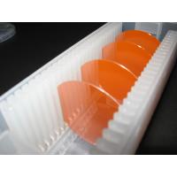
| Package | Membrance box |
Conductive Nb doped SrTiO3 Wafer
Single crystal SrTiO3 can exhibit electric conductive by doping Nb element , different doped concentration will change resistivity range from 0.001 to 0.1 ohm-cm , and this will be of benefit to some thin film growth application .
| Growth | Flame fusion ( Verneuil ) method |
|---|---|
| Diameter | Ø 1" |
| Size | 5 x 5 / 10 x 10 / 20 x 20 mm |
| Thickness | 0.5 mm / 1 mm |
| Orientation | <100> / <110> / <111> |
| Dopant | Nb ( Niobium ) |
| Concentration | 0.7 wt % |
| Resistivity | ~ 0.007 ohm-cm |
| Mobility | ~ 8.5 cm2 / v.s. |
| Surface | one side polished / two sides polished |
| TTV | <= 10 um |
| Roughness | Ra <= 5 A |
| Package | Membrance box |


