
|
|
[China]

Trade Verify
Address: Address:Room624,Fangdichan development building,Guicheng south,Nanhai,Foshan,China
Contact name:Tracy

ONESEINE TECHNOLOGY CO.,LTD |
|
Verified Suppliers
|
|
|
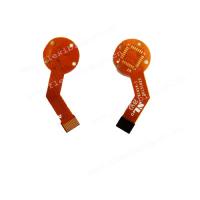
Efficient One Layer ENIG Jlcpcb Flexible Pcb Flex Pcb Prototyping
Product des.
PCB layer:1
PCB material:Polymide
Surface finish:ENIG
Board size:8*3CM
Board thickness:0.1MM
Flexible circuit boards, also known as "soft boards," are printed circuits made of flexible insulating substrates. Flexible circuits provide excellent electrical performance, which can meet the design needs of smaller and higher density installations, as well as help reduce assembly processes and enhance reliability. Flexible circuit boards are the only solution to meet the miniaturization and mobility requirements of electronic products. It can be freely bent, wound, and folded, and can withstand millions of dynamic bends without damaging the wires. It can be arranged according to spatial layout requirements, and can move and expand freely in three-dimensional space, achieving the integration of component assembly and wire connection; Flexible circuit boards can greatly reduce the volume and weight of electronic products, making them suitable for the development of electronic products towards high-density, miniaturization, and high reliability.
Rigid-flex pcb circuits
Rigid-flex circuits are a hybrid construction flex circuit consisting of rigid and flexible substrates which are laminated together into a single structure. Rigid-flex circuits should not be confused with rigidized flex constructions, which are simply flex circuits to which a stiffener is attached to support the weight of the electronic components locally. A rigidized or stiffened flex circuit can have one or more conductor layers. Thus while the two terms may sound similar, they represent products that are quite different.
The layers of a rigid flex are also normally electrically interconnected by means of plated through holes. Over the years, rigid-flex circuits have enjoyed tremendous popularity among military product designer, however the technology has found increased use in commercial products. While often considered a specialty product for low volume applications because of the challenges, an impressive effort to use the technology was made by Compaq computer in the production of boards for a laptop computer in the 1990s. While the computer's main rigid-flex PCBA did not flex during use, subsequent designs by Compaq utilized rigid-flex circuits for the hinged display cable, passing 10s of 1000s of flexures during testing. By 2013, the use of rigid-flex circuits in consumer laptop computers is now common.
Rigid-flex boards are normally multilayer structures; however, two metal layer constructions are sometimes used.

FPC Manufacturing
Flexible printed circuits (FPC) are made with a photolithographic technology. An alternative way of making flexible foil circuits or flexible flat cables (FFCs) is laminating very thin (0.07 mm) copper strips in between two layers of PET. These PET layers, typically 0.05 mm thick, are coated with an adhesive which is thermosetting, and will be activated during the lamination process. FPCs and FFCs have several advantages in many applications:
Tightly assembled electronic packages, where electrical connections are required in 3 axes, such as cameras (static application).
Electrical connections where the assembly is required to flex during its normal use, such as folding cell phones (dynamic application).
Electrical connections between sub-assemblies to replace wire harnesses, which are heavier and bulkier, such as in cars, rockets and satellites.
Electrical connections where board thickness or space constraints are driving factors.
Single-sided flex PCB circuits
Single-sided flexible circuits have a single conductor layer made of either a metal or conductive (metal filled) polymer on a flexible dielectric film. Component termination features are accessible only from one side. Holes may be formed in the base film to allow component leads to pass through for interconnection, normally by soldering. Single sided flex circuits can be fabricated with or without such protective coatings as cover layers or cover coats, however the use of a protective coating over circuits is the most common practice. The development of surface mounted devices on sputtered conductive films has enabled the production of transparent LED Films, which is used in LED Glass but also in flexible automotive lighting composites
Double-sided flex pcb circuits
Double-sided flex circuits are flex circuits having two conductor layers. These flex circuits can be fabricated with or without plated through holes, though the plated through hole variation is much more common. When constructed without plated through holes and connection features are accessed from one side only, the circuit is defined as a "Type V (5)" according to military specifications. It is not a common practice but it is an option. Because of the plated through hole, terminations for electronic components are provided for on both sides of the circuit, thus allowing components to be placed on either side. Depending on design requirements, double-sided flex circuits can be fabricated with protective coverlayers on one, both or neither side of the completed circuit but are most commonly produced with the protective layer on both sides. One major advantage of this type of substrate is that it allows crossover connections to be made very easy. Many single sided circuits are built on a double sided substrate just because they have one of two crossover connections. An example of this use is the circuit connecting a mousepad to the motherboard of a laptop. All connections on that circuit are located on only one side of the substrate, except a very small crossover connection which uses the second side of the substrate
Multilayer flex pcb circuits
Flex circuits having three or more layers of conductors are known as multilayer flex circuits. Commonly the layers are interconnected by means of plated through holes, though this is not a requirement of the definition for it is possible to provide openings to access lower circuit level features. The layers of the multilayer flex circuit may or may not be continuously laminated together throughout the construction with the obvious exception of the areas occupied by plated through-holes. The practice of discontinuous lamination is common in cases where maximum flexibility is required. This is accomplished by leaving unbonded the areas where flexing or bending is to occur.


