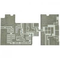
Taconic 2 Layer PCB High Frequency Circuit Boards Prototype
PCB details:
Number of layers: 2
Material: Taconic
Board thickness: 2.0mm
Surface treatment: Immersion gold
Minimum aperture: 0.20mm
Outer line width/line spacing: 5/5mil
Inner line width/line spacing: 4/4mil
Features: high frequency circuit board
High frequency PCB description:
High-frequency PCB (Printed Circuit Board) refers to a type of PCB
that is designed to handle high-frequency signals, typically in the
radio frequency (RF) and microwave ranges. These PCBs are
engineered to minimize signal loss, maintain signal integrity, and
control impedance at high frequencies.
Here are some key considerations and features of high-frequency
PCBs:
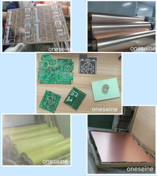
Material Selection: High-frequency PCBs often use specialized
materials with low dielectric constant (Dk) and low dissipation
factor (Df). Common materials include PTFE
(Polytetrafluoroethylene), FR-4 with enhanced properties, and
specialized laminates like Rogers or Taconic.
Controlled Impedance: Maintaining consistent impedance is crucial
for high-frequency signals. High-frequency PCBs employ controlled
impedance routing, which involves precise trace widths, spacing,
and dielectric thickness to achieve the desired characteristic
impedance.
Signal Integrity: High-frequency signals are susceptible to noise,
reflections, and losses. PCB design techniques such as proper
ground plane placement, signal return paths, and controlled
crosstalk are employed to minimize signal degradation and maintain
signal integrity.
Transmission Lines: High-frequency PCBs often incorporate
transmission lines, such as microstrip or stripline, to carry the
high-frequency signals. These transmission lines have specific
geometries to control impedance and minimize signal loss.
Via Design: Vias can impact signal integrity at high frequencies.
High-frequency PCBs may use techniques like back drilling or buried
vias to minimize signal reflections and maintain signal integrity
across layers.
Component Placement: Careful consideration is given to component
placement to minimize signal path lengths, reduce parasitic
capacitance and inductance, and optimize signal flow.
Shielding: To minimize electromagnetic interference (EMI) and RF
leakage, high-frequency PCBs may employ shielding techniques such
as copper pours, ground planes, or metal shielding cans.
High-frequency PCBs find applications in various industries,
including wireless communication systems, aerospace, radar systems,
satellite communication, medical devices, and high-speed data
transmission.
Designing and manufacturing high-frequency PCBs require specialized
skills, knowledge, and simulation tools to ensure the desired
performance at high frequencies. It is often recommended to work
with experienced PCB designers and manufacturers who specialize in
high-frequency applications.