

Active Member
|
[China]

Address: #506B, Henghui Business Center, No.77, Lingxia Nan Road, High Technology Zone, Huli, Xiamen 361006, China
Contact name:

XIAMEN POWERWAY ADVANCED MATERIAL CO., LTD. |
|
|
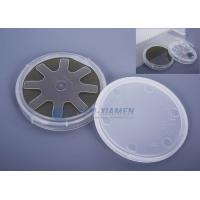
C(0001) 4H Semi-Insulating SiC Dummy Grade,4”Size -Powerway Wafer
PAM-XIAMEN provides high quality single crystal SiC (Silicon Carbide)waferfor electronic and optoelectronic industry. SiC wafer is a next generation semiconductor materialwith unique electrical properties and excellent thermal properties for high temperature and high power device application. SiC wafer can be supplied in diameter 2~6 inch, both 4H and 6H SiC , N-type , Nitrogen doped , and semi-insulating type available.
Please contact us for more information
SILICON CARBIDE MATERIAL PROPERTIES
| Polytype | Single Crystal 4H | Single Crystal 6H |
| Lattice Parameters | a=3.076 Å | a=3.073 Å |
| c=10.053 Å | c=15.117 Å | |
| Stacking Sequence | ABCB | ABCACB |
| Band-gap | 3.26 eV | 3.03 eV |
| Density | 3.21 · 103 kg/m3 | 3.21 · 103 kg/m3 |
| Therm. Expansion Coefficient | 4-5×10⁻⁶/K | 4-5×10⁻⁶/K |
| Refraction Index | no = 2.719 | no = 2.707 |
| ne = 2.777 | ne = 2.755 | |
| Dielectric Constant | 9.6 | 9.66 |
| Thermal Conductivity | 490 W/mK | 490 W/mK |
| Break-Down Electrical Field | 2-4 · 108 V/m | 2-4 · 108 V/m |
| Saturation Drift Velocity | 2.0 · 105 m/s | 2.0 · 105 m/s |
| Electron Mobility | 800 cm2/V·S | 400 cm2/V·S |
| hole Mobility | 115 cm2/V·S | 90 cm2/V·S |
| Mohs Hardness | ~9 | ~9 |
4H Semi-Insulating SiC Dummy Grade,4”Size
| SUBSTRATE PROPERTY | S4H-51-SI-PWAM-250 S4H-51-SI-PWAM-330 S4H-51-SI-PWAM-430 |
| Description | Dummy Grade 4H SEMI Substrate |
| Polytype | 4H |
| Diameter | (50.8 ± 0.38) mm |
| Thickness | (250 ± 25) μm (330 ± 25) μm (430 ± 25) μm |
| Resistivity (RT) | >1E5 Ω·cm |
| Surface Roughness | < 0.5 nm (Si-face CMP Epi-ready); <1 nm (C- face Optical polish) |
| FWHM | <50 arcsec |
| Micropipe Density | A+≤1cm-2 A≤10cm-2 B≤30cm-2 C≤50cm-2 D≤100cm-2 |
| Surface Orientation | |
| On axis <0001>± 0.5° | |
| Off axis 3.5° toward <11-20>± 0.5° | |
| Primary flat orientation | Parallel {1-100} ± 5° |
| Primary flat length | 16.00 ± 1.70 mm |
| Secondary flat orientation Si-face:90° cw. from orientation flat ± 5° | |
| C-face:90° ccw. from orientation flat ± 5° | |
| Secondary flat length | 8.00 ± 1.70 mm |
| Surface Finish | Single or double face polished |
| Packaging | Single wafer box or multi wafer box |
| Usable area | ≥ 90 % |
| Edge exclusion | 1 mm |
FAQ:
Question: I am looking for 4H semi-insulating type SiC wafer high transparency grade, 2MM thickness, with double sided polish. The transparency of wafers I currently have and want to target is 65-70% transparency at 1064 nm wavelength. I have used semi-insulating with high transparency but could switch to N-type if it is high transparency at 65-70%. We are using it as a transparent heat spreader and in the infrared emission microscopy method (IREM).I would prefer wafers with a diameter of 4” (100MM) but would be interested in 3” as well.
Answer:4” (100MM) 4H semi-insulating type SiC wafer high transparency grade, 0.5MM thickness, with double sided smooth polish. We ever tested them in this thickness 65-70% transparency at 1064nm wavelength. Research I have done indicates N-type is not very transparent at 1064 nm (~30%).
SiC crystal growth
Bulk crystal growth is the technique for fabrication of single crystalline substrates , making the base for further device processing.To have a breakthrough in SiC technology obviously we need production of SiC substrate with a reproducible process.6H- and 4H- SiC crystals are grown in graphite crucibles at high temperatures up to 2100—2500°C. The operating temperature in the crucible is provided either by inductive (RF) or resistive heating. The growth occurs on thin SiC seeds. The source represents polycrystalline SiC powder charge. The SiC vapor in the growth chamber mainly consists of three species, namely, Si, Si2C, and SiC2, which are diluted by carrier gas, for example, Argon. The SiC source evolution includes both time variation of porosity and granule diameter and graphitization of the powder granules.
SiC-Selective Doping: Ion Implantation
The fact that diffusion coefficients of most SiC dopants are negligibly small (at
1800°C) is excellent for maintaining device junction stability, because dopants do not undesirably diffuse as the device is operated long term at high temperatures. Unfortunately, this characteristic also largely (except for B at extreme temperatures ) precludes the use of conventional dopant diffusion, a highly useful technique widely employed in silicon microelectronics manufacturing, for patterned doping of SiC. Laterally patterned doping of SiC is carried out by ion implantation. This somewhat restricts the depth that most dopants can be conventionally implanted to <1 μm using conventional dopants and implantation equipment. Compared to silicon processes, SiC ion implantation requires a much higher thermal budget to achieve acceptable dopant implant electrical activation. Summaries of ion implantation processes for various dopants can be found in . Most of these processes are based on carrying out implantation at temperatures ranging from room temperature to 800°C using a patterned (sometimes high-temperature) masking material. The elevated temperature during implantation promotes some lattice self-healing during
the implant, so that damage and segregation of displaced silicon and carbon atoms does not become
excessive, especially in high-dose implants often employed for ohmic contact formation. Co-implantation
of carbon with dopants has been investigated as a means to improve the electrical conductivity of the more
heavily doped implanted layers .
Following implantation, the patterning mask is stripped and a higher temperature (~1200 to 1800°C)
anneal is carried out to achieve maximum electrical activation of dopant ions. The final annealing
conditions are crucial to obtaining desired electrical properties from ion-implanted layers. At higher
implant anneal temperature, the SiC surface morphology can seriously degrade . Because sublimation
etching is driven primarily by loss of silicon from the crystal surface, annealing in silicon overpressures
can be used to reduce surface degradation during high-temperature anneals . Such overpressure can
be achieved by close-proximity solid sources such as using an enclosed SiC crucible with SiC lid and/or
SiC powder near the wafer, or by annealing in a silane-containing atmosphere. Similarly, robust deposited
capping layers such as AlN and graphite, have also proven effective at better preserving SiC surface
morphology during high-temperature ion implantation annealing .
As evidenced by a number of works, the electrical properties and defect structure of 4H-SiC doped
by ion implantation and annealing are generally inferior to SiC doped in-situ during epitaxial
growth . Naturally, the damage imposed on the SiC lattice roughly scales with implantation dose. Even
though reasonable electrical dopant activations have been achieved, thermal annealing processes
developed to date for SiC have not been able to thoroughly repair all damage imposed on the
crystal lattice by higher-dose ion implantations (such as those often used to form heavily doped layers
in preparation of ohmic contact formation, Section 5.5.3). The degraded crystal quality of highly
implanted SiC layers has been observed to degrade carrier mobilities and minority carrier lifetimes,
thereby causing significant degradation to the electrical performance of some devices . Until
large further improvements to ion-implanted doping of SiC are developed, SiC device designs will have
to account for nonideal behavior associated with SiC-implanted layers.
 4H Semi-Insulating SiC Dummy Grade,4”Size -Powerway Wafer")
 4H Semi-Insulating SiC Dummy Grade,4”Size -Powerway Wafer")
 4H Semi-Insulating SiC Dummy Grade,4”Size -Powerway Wafer")
 4H Semi-Insulating SiC Dummy Grade,4”Size -Powerway Wafer")
 4H Semi-Insulating SiC Dummy Grade,4”Size -Powerway Wafer")
 4H Semi-Insulating SiC Dummy Grade,4”Size -Powerway Wafer")