

Active Member
|
[China]

Address: #506B, Henghui Business Center, No.77, Lingxia Nan Road, High Technology Zone, Huli, Xiamen 361006, China
Contact name:

XIAMEN POWERWAY ADVANCED MATERIAL CO., LTD. |
|
|
N Type , Te-Doped GaSb Wafer , 2”, Test Grade -Wafer Company
PAM-XIAMEN provides single crystal GaSb(Gallium Antimonide) wafer
growth by Liquid Encapsulated Czochralski ( LEC ) method.
GaSb(Gallium Antimonide) can be supplied as wafers with as-cut,
etched or polished finishes and are available in a wide range of
carrier concentration, diameter and thickness. PAM-XIAMEN can
provide epi ready grade GaSb wafer for your MOCVD & MBE
epitaxial application .Please contact our engineer team for more
wafer information.
| 2" GaSb Wafer Specification | ||
| Item | Specifications | |
| Dopant | Tellurium | |
| Conduction Type | N-type | |
| Wafer Diameter | 2" | |
| Wafer Orientation | (100)±0.5° | |
| Wafer Thickness | 500±25um | |
| Primary Flat Length | 16±2mm | |
| Secondary Flat Length | 8±1mm | |
| Carrier Concentration | (1-20)x1017cm-3 | |
| Mobility | 2000-3500cm2/V.s | |
| EPD | <2x103cm-2 | |
| TTV | <10um | |
| BOW | <10um | |
| WARP | <12um | |
| Laser Marking | upon request | |
| Suface Finish | P/E, P/P | |
| Epi Ready | yes | |
| Package | Single wafer container or cassette | |
Band structure and carrier concentration of GaSb Wafer include Basic Parameters,Temperature, Dependences,Dependence of the Energy Gap on Hydrostatic Pressure, Effective Masses, Donors and Acceptors
Basic Parameters
| Energy gap | 0.726 eV |
| Energy separation (EΓL) between Γ and L valleys | 0.084 eV |
| Energy separation (EΓX) between Γ and X valleys | 0.31 eV |
| Energy spin-orbital splitting | 0.80 eV |
| Intrinsic carrier concentration | 1.5·1012 cm-3 |
| Intrinsic resistivity | 103 Ω·cm |
| Effective conduction band density of states | 2.1·1017 cm-3 |
| Effective valence band density of states | 1.8·1019 cm-3 |
 | Band structure and carrier concentration of GaSb. 300 K Eg= 0.726 eV EL = 0.81 eV EX = 1.03 eV Eso = 0.8 eV |
Eg = 0.813 - 3.78·10-4·T2/(T+94) (eV),
where T is temperature in degrees K (0 < T < 300).
EL = 0.902 - 3.97·10-4·T2/(T+94) (eV)
EX = 1.142 - 4.75·10-4·T2/(T+94) (eV)
Nc = 4.0·1013·T3/2 (cm-3)
Nc = 4.0·1013·T3/2 (cm-3)
Nv = 3.5·1015·T3/2 (cm-3)
 | The temperature dependences of the intrinsic carrier concentration. |
Eg = Eg(0) + 14.5·10-3P (eV)
EL = EL(0) + 5.0·10-3P (eV)
EX = EX(0) - 1.5·10-3P (eV),
where P is pressure in kbar.
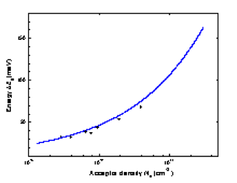 | Energy gap narrowing versus acceptor acceptor doping density. Curve is calculated for p-GaSb according to Points show experimental results |
Eg = 13.6·10-9·Nd1/3 + 1.66·10-7·Nd1/4 + 119·10-12·Nd1/2 (eV)
Eg = 8.07·10-9·Na1/3 + 2.80·10-7·Na1/4+ 4.12·10-12·Na1/2 (eV)
| For Γ-valley | mΓ = 0.041mo |
| In the L- valley the surfaces of equal energy are ellipsoids | |
| ml= 0.95mo | |
| mt= 0.11mo | |
| Effective mass of density of states | |
| mL= 16(mlmt2)1/3= 0.57mo | |
| In the X- valley the surfaces of equal energy are ellipsoids | |
| ml= 1.51mo | |
| mt= 0.22mo | |
| Effective mass of density of states | |
| mX= 9(mlmt2)1/3= 0.87mo | |
| Heavy | mh = 0.4mo |
| Light | mlp = 0.05mo |
| Split-off band | mso = 0.14mo |
| Effective mass of density of states | mv = 0.8mo |
| Effective mass of density of conductivity | mvc = 0.3mo |
 | The diagram of IV group donor states |
| Te(L) | Te(X) | Se(L) | Se(X) | S(L) | S(X) |
| ~0.02 | ≤0.08 | ~0.05 | ~0.23 | ~0.15 | ~0.30 |
For typical donor concentrations Nd≥ 1017 cm-3 the shallow donor states connected with Γ-valley did not appear.
The dominant acceptor of undoped GaSb seems to be a native defect.
This acceptor is doubly ionizable
| Ea1 | Ea2 | Si | Ge | Zn |
| 0.03 | 0.1 | ~0.01 | ~0.009 | ~0.037 |
Are You Looking for an GaSb substrate?
PAM-XIAMEN is proud to offer Gallium antimonide substrate for all
different kinds of projects. If you are looking for GaSb wafers,
send us enquiry today to learn more about how we can work with you
to get you the GaSb wafers you need for your next project. Our
group team is looking forward to providing both quality products
and excellent service for you!


