
|
|
[China]

Trade Verify
Address: Rm5-616,No.851,Dianshanhu avenue, Qingpu area,Shanghai city,CHINA
Contact name:Wang

SHANGHAI FAMOUS TRADE CO.,LTD |
|
Verified Suppliers
|
|
|
2inch ,4inch Gallium Nitride AlN template wafer on sapphire or sic substrates,HVPE Gallium Nitride wafer,AlN templates
Forbidden band width (light emitting and absorption) cover the ultraviolet, visible light and infrared.
| Product | Aluminum nitride (AlN) film | ||||||||||||
| Product Description: | AllN Epitxial proposed model saphhire hydride vapor phase epitaxy (HVPE) method. Aluminum nitride film is also cost-effective way to replace the aluminum nitride single crystal substrate. Branch Crystal sincerely welcome your inquiry! | ||||||||||||
| Technical parameters: |
| ||||||||||||
| Specifications: | 10x10x0.5mm, 10x10x1mm, dia2 "x1mm; Can be customized according to customer demand special orientation and size. | ||||||||||||
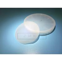
| Standard Packaging: | 1000 clean room, 100 clean bag or single box packaging |

GaN can be used in many areas such as LED display, High-energy
Detection and Imaging,
Laser Projection Display, Power Device, etc.
Specifications:
| 4” AlN Templates | 2-4inch size also ok | |
| Item | AlN-T | |
| Dimensions | Ф 100±0.3mm | |
| Substrate | Sapphire, SiC, GaN | |
| Thickness | 1000nm+/- 10% (AlN thickness) | |
| Orientation | C-axis(0001) ± 1° | |
| Conduction Type | Semi-Insulating | |
| Dislocation Density | XRD FWHM of (0002) < 200 arcsec. | |
| XRD FWHM of (10-12) < 1000 arcsec | ||
| Useable Surface Area | > 80% | |
| Polishing | Standard: SSP | |
| Option: DSP | ||
| Package | Packaged in a class 100 clean room environment, in cassettes of 25pcs or single wafer containers, under a nitrogen atmosphere. or single cassettes. | |
Other size aslike 5x5mm,10x10mm,2inch ,3inch also can be customized.
About Our Team
ZMKJ locates in the city of Shanghai, Which is the best city of China,
and our factory is founded in Wuxi city in 2014, but in the semiconductor material,
have the good experience for almost 10years.
We specialize in processing a varity of materials into
wafers, substrates and custiomized optical glass parts.components
widely used in electronics, optics, optoelectronics and many other
fields. We also have been working closely with many domestic and
oversea universities, research institutions and companies, provide
customized products and services for their R&D projects.
It's our vision to maintaining a good
relationship of cooperation with our all customers by our good
reputatiaons.


