

Active Member
|
[China]

Address: 3rd Building,Xinwuyuan Industrial Park, Difu Road,Gushu,Xixiang,Bao'an District,Shenzhen,China.
Contact name:PCB INQUIRY

Foisontech Corporation Co., Limited |
|
|
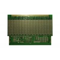
Double Sided PCB Circuit with RoHS for Customized Electronics Printed Circuit Board
For Multilayer PCB Board manufacturing, FOISON PCB has been meet with RoHS and UL compliance. The layer count of this multilayer PCB Circuit Board is 6 layers and the board thickness is 1.2 mm with blue solder mask. And the surface treatment is OSP, which help to protect the PCB bared copper from oxidation. While the minimum aperture is 0.2 mm and the line width and space is 0.1 mm.
How to get quick quotation?
![]()
| Step 1 Please send us Gerber file with these format: .CAD / .Gerber / .PCB / .DXP / .P-CAD, etc | ||||||||||||||||||||
| Step 2 Also please provide us the below details for quick quotation: | ||||||||||||||||||||
Board material: Fr - 4 / CEM - 1 / CEM - 3 / 22F / Fr - 1 / others | ||||||||||||||||||||
| Material brand: SY / KB / Rogers (optional) | ||||||||||||||||||||
| Material Specification:High Tg / copper based / aluminum based or others (optional) | ||||||||||||||||||||
| Board thickness: 0.1 - 6.0 mm | ||||||||||||||||||||
| Copper thickness: 0.05 Oz - 8 Oz ( 17 um - 288 um ) | ||||||||||||||||||||
| Surface Treatment: OSP / ENIG / HASL / Lead Free HASL / Immersion Tin / Immersion Sin | ||||||||||||||||||||
| Color of solder mask and silk print: Green / red / blue / black / white / yellow ,etc | ||||||||||||||||||||
| Board size and quantity | ||||||||||||||||||||
If you don't have Gerber file, please provide us the imfomation as step 2 or post your PCB Board to us for clone.
| ||||||||||||||||||||
SAMPLE:
| ||||||||||||||||||||
| ||||||||||||||||||||
| Layer count | Sample lead time/workday | Batch lead time/workday |
| 1-2L | 2 | 6 |
| 4L | 5 | 8 |
| 6L | 5 | 9 |
| 8L | 6 | 10 |
| 10L | 8 | 10 |
| 12L | 8 | 12 |
| 14L | 10 | 15 |
| 16L | 10 | 18 |
| 18-40L (Up to difficulty) | at least 18 | at least 24 |
| P.S. For HDI, Blind/Buried Hole PCB: Regular Lead Time + 3 workdays | ||
Q1: I am used to designing in metric units while the website is specified in imperial units.
A: When requesting an online quote, the quote form can handle mm units as well as inches for dimensions.
Q2: How do I specify internal cutouts/milling in my design?
A: All internal cutouts/slots/milling should be specified on the same layer is the board outline. The the minimum routable slot size is 32 mils. During order time, please state this requirement in the "Special Request" section so that our CAM engineers is aware of it. This is not something we encounter
Q3: What are the available holes sizes?
A: 14 mils to 150 mils - 1 mil increments 150 mils to 200 mils - 5 mil increments above 200 mils - holes would be routed out We only use drills in imperial units. Files submitted in metric units (mm) would be converted to imperial units (mils) and rounded up to the next mil.
Now send us your inquiry, and you will be replied within 8 hours!
Little knowledge - Consideration about PCB fabrication
When placed an order of PCBs (printed circuit boards), you should
spend time to considerate the basic factors including PCB board
substrate material, layer count, board size, board thickness,
copper thickness, surface finish, solder mask, silkscreen, blind
vias, buried vias, through-hole plating, SMT and so on. When all
the factors are checked and confirmed with the engineers, we highly
recommended sample tested before the real fabrication of your PCB
boards. If all things go well, fabrication could be started right
away. However, it may need to do some modification if customer is
not satisfied with the sample.


