

Active Member
|
[China]

Address: 3rd Building,Xinwuyuan Industrial Park, Difu Road,Gushu,Xixiang,Bao'an District,Shenzhen,China.
Contact name:PCB INQUIRY

Foisontech Corporation Co., Limited |
|
|
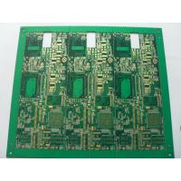
Quick Turn High Density Multilayer Prototype PCB Boards FR4 Immersion Gold
Description
1. Professional manufacturer of PCB and PCB assembly specialized in single-sided PCB, double-sided PCB, multilayer PCB, PCB layout and design and PCB assembly
2. Material Type: FR4,non-halogen material ,Aluminium Base,Cooper Base,high frequency material ,Thick copper foil,94-V0(HB),PI Material,HIGH TG:SL S1000-2,ITEQ:IT180
3. Surface treatment: HAL,Immersion Gold,Immersion Tin,Immersion silver,Gold Finger,OSP,HAL(Immersion Gold,OSP,Immersion silver,Immersion Tin)+Gold Finger
| High precision prototype | PCB bulk production | ||
| Max Layers | 1-28 layers | 1-14 layers | |
| MIN Line width(mil) | 3mil | 4mil | |
| MIN Line space(mil) | 3mil | 4mil | |
| Min via (mechanical drilling) | Board thickness≤1.2mm | 0.15mm | 0.2mm |
| Board thickness≤2.5mm | 0.2mm | 0.3mm | |
| Board thickness>2.5mm | Aspect Ration≤13:1 | Aspect Ration≤13:1 | |
| Aspect Ration | Aspect Ration≤13:1 | Aspect Ration≤13:1 | |
| Board thickness | MAX | 8mm | 7mm |
| MIN | 2 layers:0.2mm;4 layers:0.35mm;6 layers:0.55mm;8 layers:0.7mm;10 layers:0.9mm | 2 layers:0.2mm;4 layers:0.4mm;6 layers:0.6mm;8layers:0.8mm | |
| MAX Board size | 610*1200mm | 610*1200mm | |
| Max copper thickness | 0.5-6oz | 0.5-6oz | |
Immersion Gold/ Gold Plated Thickness | Immersion Gold:Au,1—8u” Gold finger:Au,1—150u” Gold Plated:Au,1—150u” Nickel Plated :50—500u” | ||
| Hole copper thick | 25um 1mil | 25um 1mil | |
| Tolerance | Board thickness | Board thickness≤1.0mm:+/-0.1mm 1.0mm<Board thickness≤2.0mm:+/-10% Board thickness>2.0mm:+/-8% | Board thickness≤1.0mm:+/-0.1mm 1.0mm<Board thickness≤2.0mm:+/-10% Board thickness>2.0mm:+/-8% |
| Outline Tolerance | ≤100mm:+/-0.1mm 100< ≤300mm:+/-0.15mm >300mm:+/-0.2mm | ≤100mm:+/-0.13mm 100< ≤300mm:+/-0.15mm >300mm:+/-0.2mm | |
| Impedance | ±10% | ±10% | |
| MIN Solder mask bridge | 0.08mm | 0.10mm | |
| Plugging Vias capability | 0.25mm--0.60mm | 0.70mm--1.00mm | |
Application
Products are applied to a wide range of High-tech industries such as: LED, telecommunication, computer application, lighting, game machine, industrial control, power, automobile and high-end consumer electronics, ect. By unremitting work and effort to the marketing, products exports to American, Canada, Europe counties, Africa and other Asia-pacific countries
Advantage
1. PCB factory directly
2. PCB Have the comprehensive quality control system
3. PCB good price
4. PCB quick turn delivery time from 48hours.
5. PCB certification(ISO/UL E354810/RoHS)
6. 8 years experience in exporting service
7. PCB is no MOQ/MOV.
8. PCB is high quality.Strict through theAOI(Automated Optical Inspection),QA/QC,fly porbe ,Etesting
| PRODUCTION CAPABILITY OF PCB | ||
PROCESS Engineer | ITEMS Item | PRODUCTION CAPABILITY Manufacturing Capability |
| Laminate | Type | FR-1,FR-5,FR-4 High-Tg,ROGERS,ISOLA,ITEQ, ALUMINUM,CEM-1,CEM-3,TACONIC,ARLON,TEFLON |
| Thickness | 0.2~3.2mm | |
| Production Type | Layer Count | 2L-16L |
| Surface Treatment | HAL,Gold Plating,Immersion Gold,OSP, Immersion Silver,Immersion Tin,Lead Free HAL | |
| Cut Lamination | Max. Working Panel size | 1000×1200mm |
| Inner Layer | Internal Core Thickness | 0.1~2.0mm |
| Internal width/spacing | Min: 4/4mil | |
| Internal Copper Thickness | 1.0~3.0oz | |
| Dimension | Board Thickness Tolerance | ±10% |
| Interlayer Alignment | ±3mil | |
| Drilling | Manufacture Panel Size | Max: 650×560mm |
| Drilling Diameter | ≧0.25mm | |
| Hole Diameter Tolerance | ±0.05mm | |
| Hole Position Tolerance | ±0.076mm | |
| Min.Annular Ring | 0.05mm | |
| PTH+Panel Plating | Hole Wall copper Thickness | ≧20um |
| Uniformity | ≧90% | |
| Outer Layer | Track Width | Min: 0.08mm |
| Track Spacing | Min: 0.08mm | |
| Pattern Plating | Finished Copper Thickness | 1oz~3oz |
| EING/Flash Gold | Nickel Thickness | 2.5um~5.0um |
| Gold Thickness | 0.03~0.05um | |
| Solder Mask | Thickness | 15~35um |
| Solder Mask Bridge | 3mil | |
| Legend | Line width/Line spacing | 6/6mil |
| Gold Finger | Nickel Thickness | ≧120u〞 |
| Gold Thickness | 1~50u〞 | |
| Hot Air Level | Tin Thickness | 100~300u〞 |
| Routing | Tolerance of Dimension | ±0.1mm |
| Slot Size | Min:0.4mm | |
| Cutter Diameter | 0.8~2.4mm | |
| Punching | Outline Tolerance | ±0.1mm |
| Slot Size | Min:0.5mm | |
| V-CUT | V-CUT Dimension | Min:60mm |
| Angle | 15°30°45° | |
| Remain Thickness Tolerance | ±0.1mm | |
| Beveling | Beveling Dimension | 30~300mm |
| Test | Testing Voltage | 250V |
| Max.Dimension | 540×400mm | |
| Impedance Control | Tolerance | ±10% |
| Aspect Ration | 12:1 | |
| Laser Drilling Size | 4mil(0.1mm) | |
| Special Requirements | Buried And Blind Via, Impedance Control, Via Plug, BGA Soldering and Gold Finger Are Acceptable | |
| OEM&ODM Service | Yes | |
How to get quick quotation?
![]()
| Step 1 Please send us Gerber file with these format: .CAD / .Gerber / .PCB / .DXP / .P-CAD, etc | ||||||||||||||||||||
| Step 2 Also please provide us the below details for quick quotation: | ||||||||||||||||||||
Board material: Fr - 4 / CEM - 1 / CEM - 3 / 22F / Fr - 1 / others | ||||||||||||||||||||
| Material brand: SY / KB / Rogers (optional) | ||||||||||||||||||||
| Material Specification:High Tg / copper based / aluminum based or others (optional) | ||||||||||||||||||||
| Board thickness: 0.1 - 6.0 mm | ||||||||||||||||||||
| Copper thickness: 0.05 Oz - 8 Oz ( 17 um - 288 um ) | ||||||||||||||||||||
| Surface Treatment: OSP / ENIG / HASL / Lead Free HASL / Immersion Tin / Immersion Sin | ||||||||||||||||||||
| Color of solder mask and silk print: Green / red / blue / black / white / yellow ,etc | ||||||||||||||||||||
| Board size and quantity | ||||||||||||||||||||
If you don't have Gerber file, please provide us the imfomation as step 2 or post your PCB Board to us for clone.
| ||||||||||||||||||||
SAMPLE:
| ||||||||||||||||||||
| ||||||||||||||||||||
| Layer count | Sample lead time/workday | Batch lead time/workday |
| 1-2L | 2 | 6 |
| 4L | 5 | 8 |
| 6L | 5 | 9 |
| 8L | 6 | 10 |
| 10L | 8 | 10 |
| 12L | 8 | 12 |
| 14L | 10 | 15 |
| 16L | 10 | 18 |
| 18-40L (Up to difficulty) | at least 18 | at least 24 |
| P.S. For HDI, Blind/Buried Hole PCB: Regular Lead Time + 3 workdays | ||
Q1: I am used to designing in metric units while the website is specified in imperial units.
A: When requesting an online quote, the quote form can handle mm units as well as inches for dimensions.
Q2: How do I specify internal cutouts/milling in my design?
A: All internal cutouts/slots/milling should be specified on the same layer is the board outline. The the minimum routable slot size is 32 mils. During order time, please state this requirement in the "Special Request" section so that our CAM engineers is aware of it. This is not something we encounter.
Q3: What are the available holes sizes?
A: 14 mils to 150 mils - 1 mil increments 150 mils to 200 mils - 5 mil increments above 200 mils - holes would be routed out We only use drills in imperial units. Files submitted in metric units (mm) would be converted to imperial units (mils) and rounded up to the next mil.
Now send us your inquiry, and you will be replied within 8 hours!
Little knowledge - Consideration about PCB fabrication
When placed an order of PCBs (printed circuit boards), you should
spend time to considerate the basic factors including PCB board
substrate material, layer count, board size, board thickness,
copper thickness, surface finish, solder mask, silkscreen, blind
vias, buried vias, through-hole plating, SMT and so on. When all
the factors are checked and confirmed with the engineers, we highly
recommended sample tested before the real fabrication of your PCB
boards. If all things go well, fabrication could be started right
away. However, it may need to do some modification if customer is
not satisfied with the sample.


