

Active Member
|
[China]

Address: Room 1204, DingCheng International Building, 518028 Futian District, SHENZHEN, CN
Contact name:Doris Guo

ChongMing Group (HK) Int'l Co., Ltd |
|
|
CY7C1328G 4-Mbit (256K x 18) Pipelined DCD Sync SRAM
Features
• Registered inputs and outputs for pipelined operation
• Optimal for performance (Double-Cycle deselect)
— Depth expansion without wait state
• 256K × 18 common I/O architecture
• 3.3V core power supply (VDD)
• 3.3V/2.5V I/O power supply (VDDQ)
• Fast clock-to-output times
— 2.6 ns (for 250-MHz device)
• Provide high-performance 3-1-1-1 access rate
• User-selectable burst counter supporting Intel® Pentium® interleaved or linear burst sequences
• Separate processor and controller address strobes
• Synchronous self-timed writes
• Asynchronous Output Enable
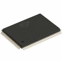
• Available in lead-free 100-Pin TQFP package
• “ZZ” Sleep Mode option
Functional Description
The CY7C1328G SRAM integrates 256K x 18 SRAM cells with advanced synchronous peripheral circuitry and a two-bit counter for internal burst operation. All synchronous inputs are gated by registers controlled by a positive-edge-triggered Clock Input (CLK). The synchronous inputs include all addresses, all data inputs, address-pipelining Chip Enable (CE1), depth-expansion Chip Enables (CE2 and CE3), Burst Control inputs (ADSC, ADSP, and ADV), Write Enables (BW[A:B], and BWE), and Global Write (GW). Asynchronous inputs include the Output Enable (OE) and the ZZ pin.
Addresses and chip enables are registered at rising edge of clock when either Address Strobe Processor (ADSP) or Address Strobe Controller (ADSC) are active. Subsequent burst addresses can be internally generated as controlled by the Advance pin (ADV).
Address, data inputs, and write controls are registered on-chip to initiate a self-timed Write cycle.This part supports Byte Write operations (see Pin Descriptions and Truth Table for further details). Write cycles can be one to two bytes wide as controlled by the byte write control inputs. GW active LOW causes all bytes to be written. This device incorporates an additional pipelined enable register which delays turning off the output buffers an additional cycle when a deselect is executed.This feature allows depth expansion without penalizing system performance.
The CY7C1328G operates from a +3.3V core power supply while all outputs operate with a +3.3V or a +2.5V supply. All inputs and outputs are JEDEC-standard JESD8-5-compatible.
Maximum Ratings
(Above which the useful life may be impaired. For user guidelines, not tested.)
Storage Temperature .................................................... –65°C to +150°C
Ambient Temperature with Power Applied.......................–55°C to +125°C
Supply Voltage on VDD Relative to GND........................... –0.5V to +4.6V
Supply Voltage on VDDQ Relative to GND ........................ –0.5V to +VDD
DC Voltage Applied to Outputs in tri-sta.................. –0.5V to VDDQ + 0.5V
DC Input Voltage ....................................................... –0.5V to VDD + 0.5V
Current into Outputs (LOW)............................................................. 20 mA
Static Discharge Voltage............................................................... > 2001V
(per MIL-STD-883,Method 3015)
Latch -up Current ........................................................................ > 200 mA
Functional Block Diagram
Package Diagram
Stock Offer (Hot Sell)
| Part NO. | Q'ty | MFG | D/C | Package |
| MC78L15ACDR2G | 30000 | ON | 10+ | SOP-8 |
| MC74HC32ADR2G | 25000 | ON | 10+ | SOP |
| MC14093BDR2G | 30000 | ON | 16+ | SOP |
| A2C11827-BD | 3000 | ST | 11+ | HSOP20 |
| LM337D2TR4 | 5991 | ON | 13+ | TO-263 |
| LTC6090CS8E | 6129 | LINEAR | 15+ | SOP |
| PC817C | 25000 | SHARP | 16+ | DIP |
| LT1170CQ | 5170 | LINEAR | 14+ | TO-263 |
| ATMXT768E-CUR | 3122 | ATMEL | 12+ | VFBGA96 |
| LM809M3X-4.63 | 10000 | NSC | 14+ | SOT-23-3 |
| PIC12F510-I/P | 5453 | MICROCHIP | 16+ | DIP |
| 30578 | 1408 | BOSCH | 10+ | QFP-64 |
| LM4040AIM3-2.5 | 10000 | NSC | 15+ | SOT-23 |
| LP38692MP-3.3 | 3843 | NSC | 15+ | SOT-223 |
| LPC4330FET256 | 2411 | 15+ | TFBGA-256 | |
| LAA120P | 2674 | CPCLARE | 15+ | SOP8 |
| MCP42010-I/SL | 5356 | MICROCHIP | 16+ | SOP |
| LM3940IMP-3.3 | 10000 | NSC | 15+ | SOT-223 |
| MAX668EUB-T | 5418 | MAXIM | 16+ | MSOP |
| MAX16054AZT+ | 6100 | MAXIM | 15+ | SOT |
| PCA9555PW | 12520 | 11+ | TSSOP |
 Pipelined DCD Sync SRAM")
 Pipelined DCD Sync SRAM")
 Pipelined DCD Sync SRAM")
 Pipelined DCD Sync SRAM")
 Pipelined DCD Sync SRAM")
 Pipelined DCD Sync SRAM")