
|
|
[China]

Trade Verify
Address: Building 11, Lane 1333, Jiangnan Avenue, Changxing Town, Chongming District, Shanghai
Contact name:Xiwen Bai (Ciel)

Shanghai GaNova Electronic Information Co., Ltd. |
|
Verified Suppliers
|
|
|
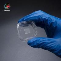
JDCD05-001-006 10*10mm2*0.5mm electronic grade single crystal diamond,N content<100ppb, XRD<0.015º Thermal conductivity 1000-2200 for heat sink
Overview
CVD diamond has long been recognized as the ultimate material in a wide variety of applications due to its extreme qualities.
For diamond CVD atomic hydrogen plays a key role. It is obtained by dissociating hydrogen molecules (H2). So, what we need is a process gas that consists mainly of hydrogen (>90 %) and a gas activation, e.g. an intense plasma or a hot filament, to break up the hydrogen molecules. Atomic hydrogen is known to selectively etch graphite and to break up double bonds thus converting graphitic bonds into diamond bonds.
Specification
| properties | Synthetic diamond | |
| Density(g/cm3) | 3.515 | Intrinsic properties |
| Young’s modulus(GaP) | 1050 |
Mechanical property |
| Hardness(GaP) | 70~120single crystal 60~100 polycrystalline | |
| Breaking strength | 2.5-3GPasingle crystal 200-1100MPa polycrystalline | |
| Fracture toughness(MPa·m1/2) | 1~8 | |
| Firction coefficient | 0.1 | |
| Thermal conductivity(300K,Wm·K) | 1000~2200 | Thermal properties |
| Coefficient of thermal expansion(×10-6/℃) | 1(room temperature) | |
| Rerfractive index(590nm) | 2.4 | Optical properties |
| Light transmittance | 225nm to far infrared | |
| Band gap width(ev) | 5.47 | Electrical properties |
| Resistivity(Ω·cm) | >1010 | |
| Electron mobility(cm2/V·S) | 4500 | |
| Hole mobility(cm2/V·S) | 3800 | |
| Dielectric constant | 5.5 | Dielectric properties |
| Dielectric losses | <2×10⁻⁴ |
About Us
We specialize in processing a variety of materials into wafers, substrates and customized optical glass parts.components widely used in electronics, optics, opto electronics and many other fields. We also have been working closely with many domestic and oversea universities, research institutions and companies, provide customized products and services for their R&D projects. It's our vision to maintaining a good relationship of cooperation with our all customers by our good reputations.
FAQ
Q: Are you trading company or manufacturer ?
We are factory.
Q: How long is your delivery time?
Generally it is 3-5 days if the goods are in stock.
or it is 7-10 days if the goods are not in stock, it is according
to quantity.
Q: Do you provide samples ? is it free or extra ?
Yes, we could offer the sample for free charge but do not pay the
cost of freight.
Q: What is your terms of payment ?
Payment <=5000USD, 100% in advance.
Paymen >=5000USD, 80% T/T in advance , balance before shippment.


