
|
|
[China]

Trade Verify
Address: Building 11, Lane 1333, Jiangnan Avenue, Changxing Town, Chongming District, Shanghai
Contact name:Xiwen Bai (Ciel)

Shanghai GaNova Electronic Information Co., Ltd. |
|
Verified Suppliers
|
|
|
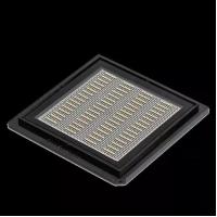
Laser Printing Laser Diode Chip Operating Temperature 15-55℃ Output Power 10W
915nm 10W COS Diode Laser Chip On Submount Design
Recent progress in high performance silicon large scale integration (Si-LSI) has faced major challenges from limitations in the bandwidth of electrical interconnects due to signal delay, and also from heating due to the large density of electrical interconnects.
Of the potential solutions to overcome these issues optical interconnects are of considerable interest since they feature very large bandwidths that could ultimately lead to more efficient ways of routing information within LSI circuits.
Optical | |
Center Wavelength | 915nm |
Output Power | 10W |
Spectral Width FWHM | ≤6nm |
Slope Efficiency | 1.0W/A |
Fast Axis Divergence | 60Deg |
Slow Axis Divergence | 11Deg |
Polarization Mode | TE |
Emitter Size | 94um |
Electrical | |
Threshold Current | 0.5A |
Operating Current | 12A |
Operating Voltage | 1.65V |
Power Conversion Efficiency | 58% |
Thermal | |
Operating Temperature | 15-55℃ |
Storage Temperature | -30-70℃ |
Wavelength Temp. Coefficient | 0.3nm/℃ |
FAQ
Q1: What payment methods do you support?
T/T and Western Union, For your Choice
Q2: How long can I receive the package?
Normally 1-2 Weeks FedEx,DHL Express,UPS,TNT
Q3: What is the lead time?
Standard product are all in stock. Shipping via Express within 3~4
working days. Customized stack need 15 working days.
Q4: Are you trading company or manufacturer?
We are manufacturer with more than 11 years of experience, and also
provide the technical solution to all customers.
Q5: Can you guarantee your quality?
Of course, we are one of top reputed manufacturers in China.
Quality for us is the most important thing, we put high value on
our reputation. Best quality is our principle all the time.


