
|
|
[China]

Trade Verify
Address: Building 11, Lane 1333, Jiangnan Avenue, Changxing Town, Chongming District, Shanghai
Contact name:Xiwen Bai (Ciel)

Shanghai GaNova Electronic Information Co., Ltd. |
|
Verified Suppliers
|
|
|
Growth Method CZ Silicon Wafer Orientation <1-0-0>,<1-1-1>,<1-1-0>
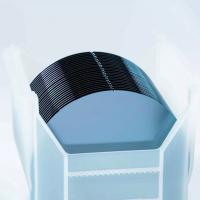
2-Inch Silicon Wafer MEMS Devices, Integrated Circuits,Dedicated Substrates For Discrete Devices
Overview
Silicon wafers after cutting have sharp edges, and they chip easily. Wafer edge is shaped to remove sharp, brittle edges; rounded edge minimizes risk for slipping, too. Edge shaping operation makes the wafer perfectly round (off-cut wafers are oval shaped after slicing), the diameter is adjusted, and orientation flat(s) or notch is dimensioned or made.
Specification
| silicon wafer | |
Diameter
| 2"/3"/4"/5"/6"/8"/12" |
| Grade | Prime |
| Growth Method | CZ |
| Orientation | <1-0-0>,<1-1-1>,<1-1-0> |
| Type/Dopant | P Type/Boron,N Type/Phos,N Type/As, N Type/Sb |
| Thickness(μm) | 279/380/525/625/675/725/775 |
| Thickness Tolerance | Standard ± 25μm,Maximum Capabilit/ies ± 5μm |
| Resistivity | 0.001-100 ohm-cm |
| Surface Finished | P/E,P/P,E/E,G/G |
| TTV(μm) | Standard <10 μm,Maximum Capabilities<5 μm |
| Bow/Warp | Standard <40 μm,Maximum Capabilities<20 μm |
| Particle | <10@0.5μm; <10@0.3μm; <10@0.2μm; |
About Us
We specialize in processing a variety of materials into wafers, substrates and customized optical glass parts.components widely used in electronics, optics, opto electronics and many other fields. We also have been working closely with many domestic and oversea universities, research institutions and companies, provide customized products and services for their R&D projects. It's our vision to maintaining a good relationship of cooperation with our all customers by our good reputations.
FAQ
Q: Are you trading company or manufacturer ?
We are factory.
Q: How long is your delivery time?
Generally it is 3-5 days if the goods are in stock.
or it is 7-10 days if the goods are not in stock, it is according
to quantity.
Q: Do you provide samples ? is it free or extra ?
Yes, we could offer the sample for free charge but do not pay the
cost of freight.
Q: What is your terms of payment ?
Payment <=5000USD, 100% in advance.
Paymen >=5000USD, 80% T/T in advance , balance before shippment.


