

Active Member
|
[China]

Address: Chengda Business Center, Rongfu Road, Fucheng Street, Longhua District, Shenzhen
Contact name:Lynn

Shenzhen Shinelink Technology Ltd |
|
|
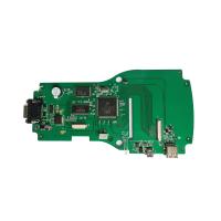
Customizable SMT PCB Assembly , Bluetooth Headset Circuit Board Assembly
This PCBA Board is assembled with FR - 4 made bare pcb board and the board thickness is 1.6 mm, copper thickness is normally 1OZ / 35 µm. Immersion gold surface treatment make the PCBa work longer and more eco-friendly. We need Gerber File & BOM List to produce your PCBa assembly order.
Files Requested For PCB Assembly Quotation
---In order to provide you with the most efficient and accurate
quote on manufacturing the requested unit, we ask that you provide
us with the following information.
1. Gerber file,PCB file,Eagle file or CAD file are all acceptable
2. A detailed bill of materials (BOM)
3. Clear pictures of PCB or PCBA sample for us
4. Quantity and delivery required
5. Test method for PCBA to guarantee 100% good quality products.
6. Schematics file for PCB design if need to do function test.
7. A sample if available for better sourcing
8. CAD files for enclosure manufacturing if required
9. A complete wiring and assembly drawing showing any special
assembly instructions if required
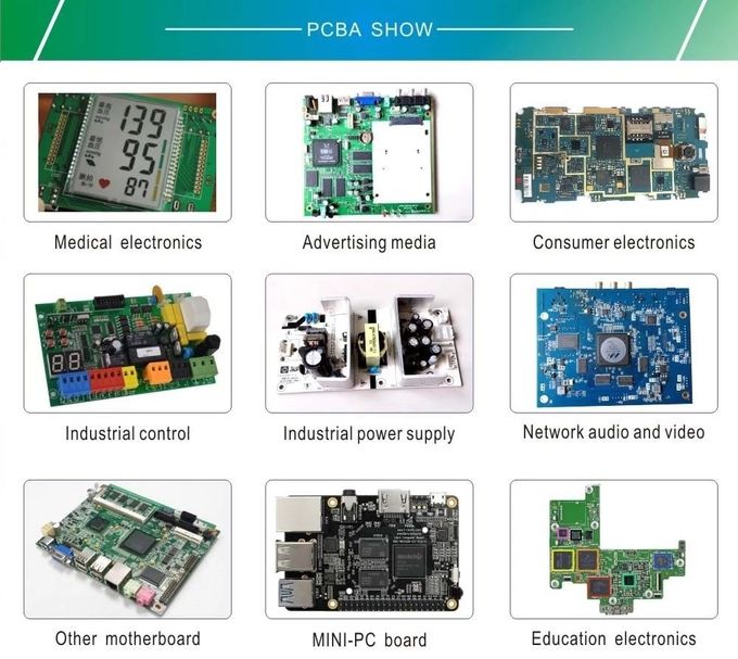
Shinelink kinds PCBA product
94V0 PCBA manufacture Scale capabilities up to
We combine advanced processes with highly skilled resources.
Keeping up with the leading advanced technology and management
system in One-stop services of PCB assembly
SMT process (RoHs Compliant) Capabilities up to:
1. 0201 Chip Size
2. 12 mils Integrated Circuit (IC) Pitch
3. Micro Ball Grid Array (BGA) – Pitch 16 mils
4. Flip Chip (Controlled Collapse Chip Connection) – Pitch 5 mils
5. Quad Flat Package (QFP) – Pitch 12 mils
THT(Wave soldering) process (RoHs Compliant) Capabilities up to:
1.Single side wave soldering
2.SMT & THT mixture process
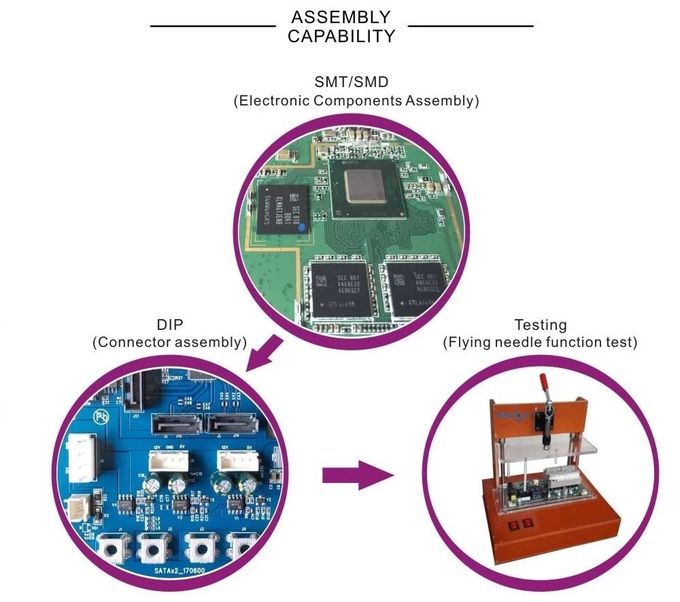
PCB Assembly Capabilities
| Turnkey PCBA | PCB+components sourcing+assembly+package |
| Assembly details | SMT and Thru-hole, ISO lines |
| Lead Time | Prototype: 15 work days. Mass order: 20~25 work days |
| Testing on products | Flying Probe Test, X-ray Inspection, AOI Test, functional test |
| Quantity | Min quantity: 1pcs. Prototype, small order, mass order, all OK |
| Files we need | PCB: Gerber files(CAM, PCB, PCBDOC) |
| Components: Bill of Materials(BOM list) | |
| Assembly: Pick-N-Place file | |
| PCB panel Size | Min size: 0.25*0.25 inches(6*6mm) |
| Max size: 20*20 inches(500*500mm) | |
| PCB Solder Type | Water Soluble Solder Paste, RoHS lead free |
| Components details | Passive Down to 0201 size |
| BGA and VFBGA | |
| Leadless Chip Carriers/CSP | |
| Double-sided SMT Assembly | |
| Fine Pitch to 0.8mils | |
| BGA Repair and Reball | |
| Part Removal and Replacement | |
| Component package | Cut Tape,Tube,Reels,Loose Parts |
| PCB assembly process | Drilling-----Exposure-----Plating-----Etaching & Stripping-----Punching-----Electrical Testing-----SMT-----Wave Soldering-----Assembling-----ICT-----Function Testing-----Temperature & Humidity Testing |
PCBA Picture

FAQ:
1. What’s the typical process flow for multi-layer PCB?
Material cutting → Inner dry film → inner etching → Inner AOI → Multi-bond→ Layer stack up Pressing → Drilling → PTH → Panel Plating → Outer Dry Film → Pattern Plating → Outer etching → Outer AOI → Solder Mask → Component Mark → Surface finish → Routing → E/T → Visual Inspection.
2. What’s the key equipments for HDI manufacturing?
Key equipment list is as following: Laser drilling machine, Pressing machine, VCP line, Automatic Exposing machine, LDI and etc.
The equipments we have are the best in the industry, laser drilling machines are from Mitsubishi and Hitachi, LDI machines are from Screen(Japan), Automatic Exposing machines are also from Hitachi, all of them make we can meet customer’s technical requirements.
3. How many types of surface finish SHINELINK can do?
SHINELINK has the full series of surface finish, such as: ENIG, OSP, LF-HASL, gold plating (soft/hard), immersion silver, Tin, silver plating, immersion tin plating, carbon ink and etc. .. OSP, ENIG, OSP + ENIG commonly used on the HDI, we usually recommend that you use a client or OSP OSP + ENIG if BGA PAD size less than 0.3 mm.
4. What’s your capability for FPC? Can SHINELINK provide SMT
service also?
SHINELINK can fabricate FPC from single layer to 8layer, the working panel size can be as large as 2000mm*240mm, please find the details in the page “Flex Capability”
We also provide SMT one stop service to customer.


