What we offer: 1) Good quality control 2) Highly competitive prices 3)
state-of-art technology products 4) Best professional team of
lifestyle consumer electronics. 5) Smooth communication 6)
Effective OEM&ODM service

|
|
[China]

Trade Verify
Address: Building D4, 3rd Floor, Unit 315, Yingzhan Industrial Park, Longtian Community, Pingshan District, Shenzhen City, Guangdong Province.
Contact name:Agnes.H

Kezhixin (Shenzhen) Technology Co., Ltd. |
|
Verified Suppliers
|
|
|
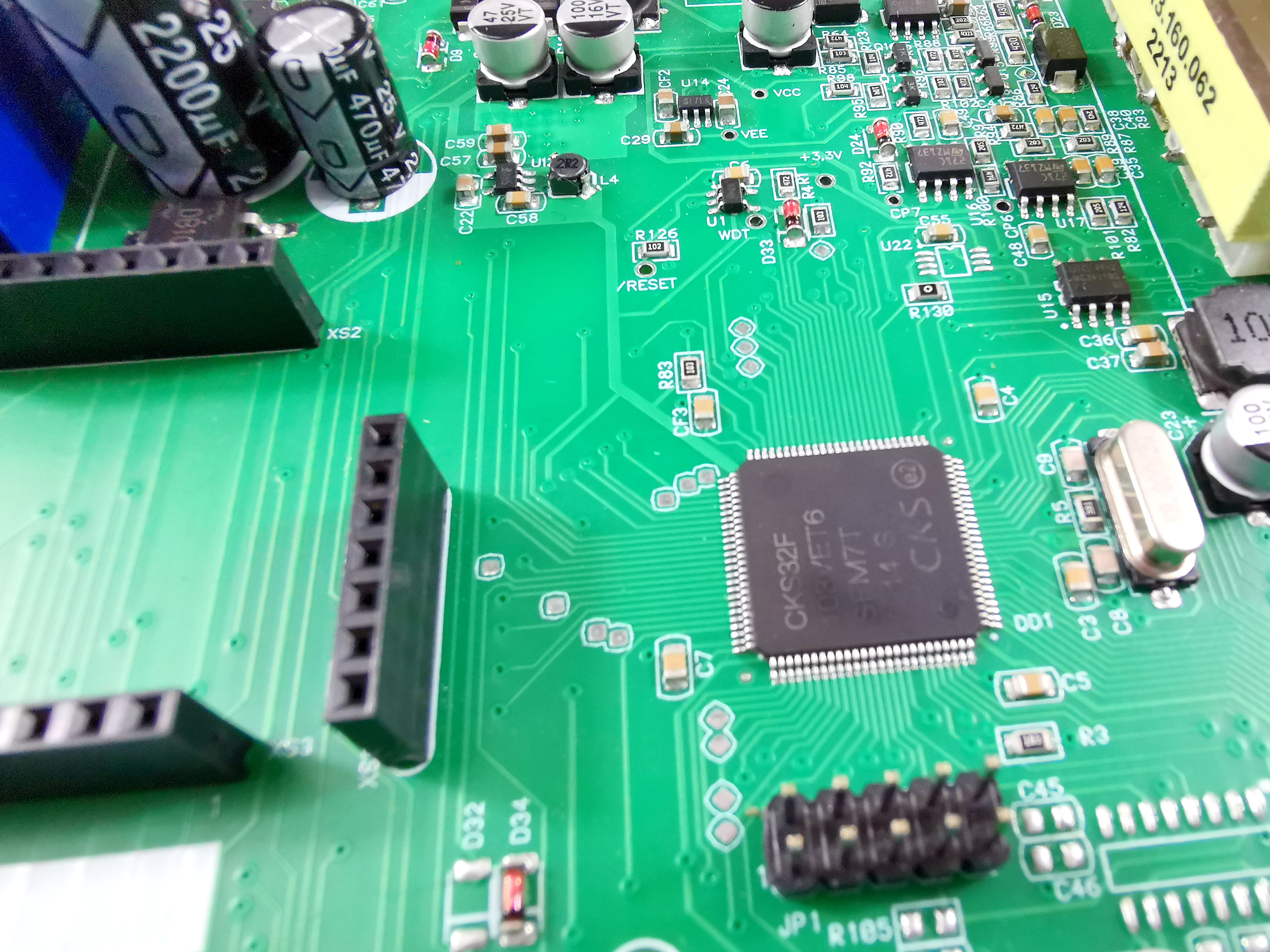
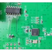
PCBA Assembly Wonderful PCB SMT Electronic Component PCBA Circuit Board PCB Assembly
PCB Technical Specification | ||||||||||
Order quantity | 1-500,000 | |||||||||
Number of layer | 1,2,4,6,up to 22 layers | |||||||||
Board material | FR-4, glass epoxy, FR4 High Tg, Rohs compliant, Aluminum, Rogers,
etc | |||||||||
PCB type | Hard, flexible, rigid-flexible | |||||||||
Shape | Any shape: Rectangular,round,slots,cutouts,complex,irregular, etc | |||||||||
Max PCB dimensions | 20inch*20inch or 500mm*500mm | |||||||||
Board thickness | 0.4~4.0mm | |||||||||
Thickness tolerance | ± 10% | |||||||||
Copper thickness | 1/2OZ 1OZ 2OZ 3OZ | |||||||||
Copper thickness tolerance | ± 0.25oz | |||||||||
Solder mask | Green, red, white, yellow, blue, black, etc | |||||||||
Silk screen | White, yellow, black, or negative, etc | |||||||||
Silk screen min line width | 0.006'' or 0.15mm | |||||||||
Surface finish | HASL, Nickle, Imm Gold, Imm Tin, Imm Silver, OSP etc | |||||||||
Min drill hole diameter | 0.01'',0.25mm.or 10 mil | |||||||||
PCB cutting | Shear,V-score,tab-routed | |||||||||
PCB Assembly Capabilities | ||||||||||
SMT Jointing Min. Space | 0201mm | |||||||||
QFP Space | Pitch 0.3mm | |||||||||
Min. Package | 201 | |||||||||
Min. Size | 2*2 inch(50*50mm) | |||||||||
Max. Size | 14*22 inch(350*550mm) | |||||||||
Placement Precision | ±0.01mm | |||||||||
Placement Precision | QFP, SOP, PLCC, BGA | |||||||||
Placement Capability | 0805, 0603, 0402, 0201 | |||||||||
PCB Lead time (workday(s)) | ||||||||||
Single, Double-sided | 4 layer | 6 layer | Over 8 layer | HDI | ||||||
Sample Lead time (Normal) | 4~5 days | 6~7 days | 7~8 days | 10~12 days | 10~12 days | |||||
Sample Lead time (Faster) | 2~3 days | 3~5 days | 6 days | 6~7 days | 12 days | |||||
Mass production lead time | 7~10 days | 10~14 days | 13-14 days | 16 days | 20 days | |||||
PCB Assembly Lead time | ||||||||||
Sample Lead time | PCB Fab+Components Sourcing+PCBA= 7~15 days according to level
difficulties. | |||||||||
Mass production lead time | PCB Fab+Components Sourcing+PCBA=14~28 daysaccording to QTY and
level difficulties. | |||||||||